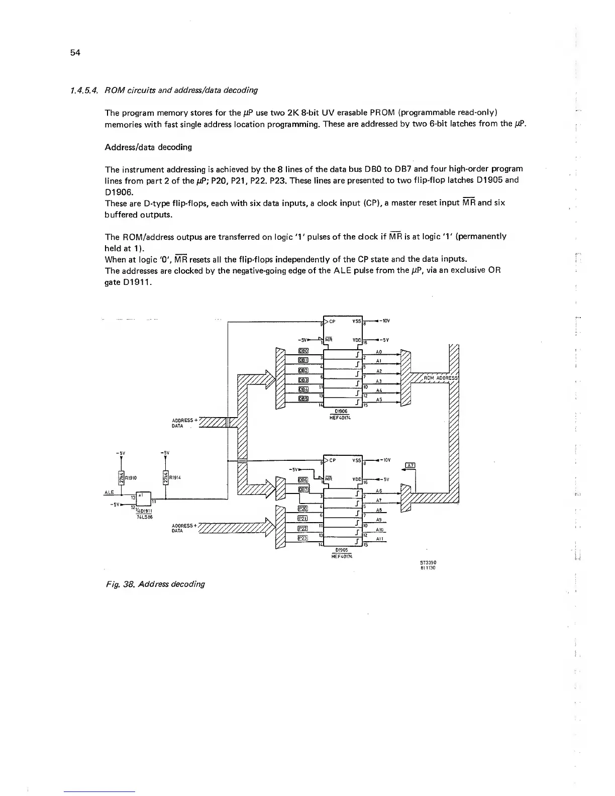
54
1. 4.5.4. ROM
circuits and address/data
decoding
The program
memory stores for the /tP use two 2K 8-bit UV
erasable PROM
(programmable
read-only)
memories
with fast single address location
programming.
These are addressed by
two
6-bit latches from
the /tP.
Address/data decoding
The
instrument
addressing is achieved
by
the
8
lines of the
data bus DBO to
DB7 and
four
high-order program
lines from part 2
of the juP; P20, P21, P22. P23.
These lines are
presented to two
flip-flop
latches D1905 and
D1906.
These are
D-type flip-flops, each with six data
inputs,
a
clock input
(CP), a
master reset input MR and six
buffered outputs.
The ROM/address
outpus are transferred on logic 'V
pulses of the clock
if MR
is at
logic
'1'
(permanently
held
at
1
).
When
at logic 'O',
MR
resets
all the flip-flops
independently of the CP
state and the data
inputs.
The addresses are
clocked
by
the negative-going edge of
the ALE pulse from
the jUP,
via an exclusive OR
gate D1911.
ST3390
811130
Fig. 38.
Address decoding