66
The table below summarizes the addresses of the areas reserved to I/O
devices, according to their communication address:
17-32 17-32 7-10 5-8 200-209
33-48 33-48 11-14 9-12 210-219
49-64 49-64 15-18 13-16 220-229
65-80 65-80 19-22 17-20 230-239
81-96 81-96 23-26 21-24 240-249
97-112 97-112 27-30 25-28 250-259
113-128 113-128 31-34 29-32 260-269
129-144 129-144 35-38 33-36 270-279
145-160 145-160 39-42 37-40 280-289
161-176 161-176 43-46 41-44 290-299
177-192 177-192 47-50 45-48 300-309
193-208 193-208 51-54 49-52 310-319
209-224 209-224 55-58 53-56 320-329
225-240 225-240 59-62 57-60 330-339
241-256 241-256 63-66 61-64 340-349
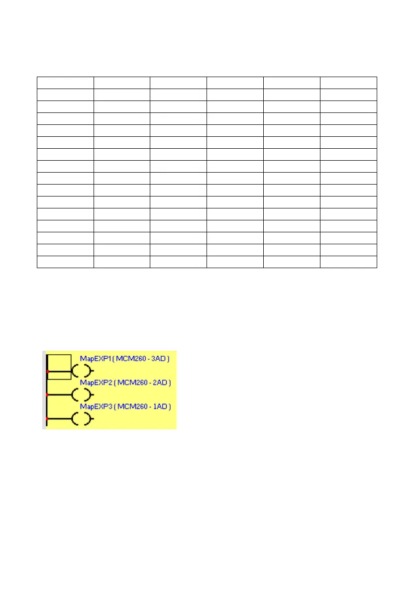
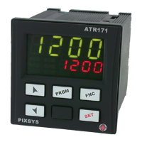
The example below shows how to activate the management of three
devices, it is possible to see that: the module with address 1 is a MCM260-
3AD, those with address 2 is a MCM260-2AD and those with address 3 is a
MCM260-1AD. Digital inputs/outputs will be available for the address
indicated near the figure.
I17..I24 e Q17..Q24
I33..I48 Q49..Q64