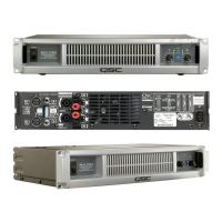
50 QSC Audio Products, LLC
high rail, then the gate drive is incorrectly turning the FET on.
Malfunctioning gate drive circuitry should be checked as descibed
under
Fault: Step won’t turn on (premature clipping)
.
Fault: Repeated FET failure
Repeated failure of a step FET is usually caused by thermal stress
because of a failure to switch fully on or off—that is, the FET
lingers in its linear region. Failures usually occur with 2-ohm loads,
when the FET’s dissipation is highest.
After replacing the FET, you should monitor the step waveform with
a large signal. Start with at light load, 8 ohms, to avoid a repeat
failure. Advance briefly to heavier loads—4 and then 2 ohms—
while closely watching the waveform. You will need to use an
isolated scope probe which allows voltage readings to be taken
with respect to the intermediate rails, or to FET sources.
Fault: Excessive step distortion (step glitch)
Close scrutiny of the distortion trace, and scope probing of the
switched waveform, will help determine the cause of excess step
distortion. The step should switch when the output voltage rises to
within 10 to 12 volts of the low rail voltage. This switching margin
should be fairly constant throughout the audio spectrum, from 20 Hz
to 20 kHz.
The switching event itself should be a fairly uniform up or down
ramp, changing at a rate of about 25 V/µs. It should therefore take
about 2 µs to complete its transition.
Fault: Step switching too close to the rail
The step switches well after the signal voltage has approached to
within 10 to 12 volts of the low rail voltage.
This will cause increased step glitch, especially at low load
impedances. If this happens at all signal frequencies, check the
reference voltages at the nodes POSREF and NEGREF.
• POSREF should be about 20 V below the +MID-RAIL node.
• NEGREF should be about 17.5 V above the -MID-RAIL node.
Confirm correct resistor values in the output voltage divider: R48–
R50 (channel 1) or R171–R173 (channel 2).
If the switching problem is present only on high frequencies, check
the value of the speed up capacitor C20 (channel 1) or C55 (channel
2) in the output voltage divider, or look for slow switching (see
Fault:
Slow or fast switching
, below).
Fault: Step chattering
If the step repeatedly switches on and off in rapid succession, it
creates an oscillation burst which increases step glitch. The
tendency is usually greater with low-frequency signals and low load
impedances. Two or three “false switches” at the step threshold on
very low frequency signals into 2-ohm loads is acceptable, but
prolonged bursts of chattering on mid or high frequencies may
cause FET failure.
To minimize chattering the step comparator has hysteresis, or
positive feedback, to slightly shift the threshold when it changes
state; when the comparator switches the step on, it shifts the “off”
threshold slightly toward zero.
• Positive step: Check the hysteresis resistor R66 (channel 1) or
R189 (channel 2).
• Negative step: Check the hysteresis resistor R69 and capacitor
C187 (channel 1) or R192 and C193 (channel 2).
Fault: Slow or fast switching
Slow switching reduces step glitch but puts more stress on the FET.
Fast switching, on the other hand, increases step glitch. The usable
range of step transition speed is about 17–27 volts/µs.
If the turn-on and turn-off slopes both appear to be equally off
speed, check the slope capacitors: C30 (positive) and C29 (negative
on channel 1, or C65 (positive) or C64 (negative) on channel 2.
If only one slope is slow, check these components and buffer
transistors:
• Positive step: R78, R79, D15, Q30, and Q31 (channel 1); R201,
R202, D40, Q75, and Q76 (channel 2).
• Negative step: R83, R84, D17, Q32, and Q33 (channel 1); R206,
R207, D42, Q77, and Q78 (channel 2).
Fault: Step FET oscillation
Certain FET types tend to oscillate at extremely high frequency
while ramping up and down. This injects interference into the
signal, effectively increasing the step glitch. Identifying such
tendencies is one of the evaluative tasks in qualifying or disqualify-
ing specific FET types. If these problems appear in any QSC
amplifier, please report it to QSC Technical Services.
Fault: Severe step oscillation
This happens generally on low frequencies with low load imped-
ances, right at the step threshold.
• Positive step: Check the hysteresis resistor R66 (channel 1) or
R189 (channel 2).
• Negative step: Check the hysteresis resistor R69 and capacitor
C187 (channel 1) or R192 and C193 (channel 2).
3.2 PL325 and PL340: Symptoms, causes, and remedies (continued)
 Loading...