4 QSC Audio Products, LLC
Tables and Figures
Chassis Assembly PL380 (120V) (QSC part # WP-038000-00) .................................................................................................................................................................... 120
Chassis Assembly PL380 (100V) (QSC part # WP-038000-01) .................................................................................................................................................................... 121
Chassis Assembly PL380 (230V) (QSC part # WP-038000-02) .................................................................................................................................................................... 122
PCB Assembly PL380 (120V) (QSC part # WP-038001-00) through January 2008 ..................................................................................................................................... 122
PCB Assembly PL380 (100V) (QSC part # WP-038001-01) through January 2008 ..................................................................................................................................... 126
PCB Assembly PL380 (230V) (QSC part # WP-038001-02) through January 2008 ..................................................................................................................................... 130
PCB Assembly PL380 (120V) (QSC part # WP-038001-00) from February 2008– ....................................................................................................................................... 134
PCB Assembly PL380 (100V) (QSC part # WP-038001-01) from February 2008– ....................................................................................................................................... 138
PCB Assembly PL380 (230V) (QSC part # WP-038001-02) from February 2008– ....................................................................................................................................... 142
Table of Contents (continued)
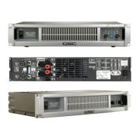
PL325 and PL340 amplifier, rear view ..................................................................................................................................................................... 2
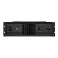
PL380 amplifier, rear view ....................................................................................................................................................................................... 2
Table 1.1. Load resistor bank switch truth table ..................................................................................................................................................... 7
Figure 1.1. Load resistor bank ................................................................................................................................................................................. 7
Figure 1.2. Use two irons......................................................................................................................................................................................... 8
Figure 1.3. Soak up solder ....................................................................................................................................................................................... 8
Figure 1.4. Apply new solder ................................................................................................................................................................................... 8
Figure 1.5. Place component ................................................................................................................................................................................... 8
Figure 1.6. Solder one end of the component ......................................................................................................................................................... 8
Figure 1.7. Solder other end .................................................................................................................................................................................... 8
Figure 1.8. The PL380 service fixture .................................................................................................................................................................... 10
Figure 1.9. Locations of Test Point A and Test Point B .......................................................................................................................................... 10
Figure 1.10. Jumpers to be removed from Test Point B ........................................................................................................................................ 11
Figure 1.11. Connecting the hookup leads ............................................................................................................................................................ 11
Figure 1.12. Schematic diagram of the PL380 service fixture .............................................................................................................................. 12
Figure 1.13. Proper IGBT drive signals (with chassis ground reference ) ............................................................................................................. 13
Figure 1.14. Proper FET gate drive signals with FETs installed (with chassis ground reference) ....................................................................... 13
Figure 2.1. Signal with 250 kHz switching noise .................................................................................................................................................. 21
Figure 2.2. Signal with switching noise filtered out ............................................................................................................................................. 21
Figure 2.3. Burst sine wave signal for 2
Ω
power testing ..................................................................................................................................... 21
Figure 2.4. Noise and distortion residual with bias properly set .......................................................................................................................... 25
Figure 3.1 IGBT gate drive waveforms .................................................................................................................................................................. 32
Figure 3.2 FET gate drive waveforms .................................................................................................................................................................... 33
Figure 3.3 Dead time between one pulse turning off and the other turning on should be about 20–30 ns at the 5 V level. ............................. 33
Figure 3.4 The clock drive logic signals................................................................................................................................................................. 33
Figure 3.5 The power supply sync pulse. .............................................................................................................................................................. 34
Figure 3.6 Triangle wave at comparator inputs (pin 2 of U8 and U28). ................................................................................................................ 35
Figure 3.7 Triangle wave with supply rails energized. .......................................................................................................................................... 35
Figure 3.8. Switching pulse at node N401 (pin 3 of U19) ..................................................................................................................................... 39
Figure 3.9: Switching signal with dead time at nodes N397 and 398 (pins 11 and 14 of U19). .......................................................................... 40
Figure 3.10. Typical crossover residual from distortion analyzer output .............................................................................................................. 41
Figure 3.11. Identify damaged transistors by measuring resistance across the collector and emitter. .............................................................. 43
Table 3.1. Clamping voltage troubleshooting ....................................................................................................................................................... 44
Table 3.2. Troubleshooting clamp malfunctions ................................................................................................................................................... 45
Figure 3.12. The overcurrent detection circuit for power supply cutback. ........................................................................................................... 46
Table 3.3. Troubleshooting clamp transistors ....................................................................................................................................................... 46
 Loading...