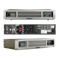
PL3 Series Service Manual 5
TD-000274-00 Rev. A
Table 3.4. Troubleshooting short circuit cutback clamping ................................................................................................................................... 47
Figure 3.13. Output signal and positive rail steps. ............................................................................................................................................... 48
Figure 3.14. Output signal and negative rail steps. .............................................................................................................................................. 48
PL325 and PL340 main circuit board, with major circuit sections shown ............................................................................................................ 53
PL325 and PL340 main circuit board, top layer ..................................................................................................................................................... 54
PL325 and PL340 main circuit board, bottom layer, mirror image ........................................................................................................................ 55
PL325 and PL340 input board, top layer ............................................................................................................................................................... 56
PL325 and PL340 input board, bottom layer, mirror image ................................................................................................................................... 57
PL380 main circuit board, with major circuit sections shown .............................................................................................................................. 58
PL380 main circuit board, detailed view ............................................................................................................................................................... 59
PL380 input board, main circuit blocks shown ...................................................................................................................................................... 59
PL380 main circuit board, top layer ....................................................................................................................................................................... 60
PL380 main circuit board, mid1 layer .................................................................................................................................................................... 61
PL380 main circuit board, mid2 layer .................................................................................................................................................................... 62
PL380 main circuit board, bottom layer ................................................................................................................................................................ 63
PL325 schematic notes .......................................................................................................................................................................................... 64
Schematic sheet INPUT, PL325 ............................................................................................................................................................................. 65
PL325 wiring diagram ............................................................................................................................................................................................ 66
PL325 schematic guide .......................................................................................................................................................................................... 67
Schematic sheet AMP CH-A, PL325...................................................................................................................................................................... 68
Schematic sheet AMP CH-B, PL325 ...................................................................................................................................................................... 69
Schematic sheet PROTECT/CONTROL, PL325 ...................................................................................................................................................... 70
Schematic sheet POWER SUPPLY, PL325 ............................................................................................................................................................. 71
PL340 schematic notes .......................................................................................................................................................................................... 72
Schematic sheet INPUT, PL340 ............................................................................................................................................................................. 73
PL340 wiring diagram ............................................................................................................................................................................................ 74
PL340 schematic guide .......................................................................................................................................................................................... 75
Schematic sheet AMP CH-A, PL340...................................................................................................................................................................... 76
Schematic sheet AMP CH-B, PL340 ...................................................................................................................................................................... 77
Schematic sheet PROTECT/CONTROL, PL340 ...................................................................................................................................................... 78
Schematic sheet POWER SUPPLY, PL340 ............................................................................................................................................................. 79
PL380 schematic notes .......................................................................................................................................................................................... 80
PL380 wiring diagram ............................................................................................................................................................................................ 81
PL380 schematic guide .......................................................................................................................................................................................... 82
Schematic sheet AMP CH-A, PL380 through January 2008 ................................................................................................................................. 83
Schematic sheet PROTECT/CONTROL, PL380 ...................................................................................................................................................... 84
Schematic sheet AMP CH-B, PL380 through January 2008 ................................................................................................................................. 85
Schematic sheet POWER SUPPLY, PL380 through January 2008 ......................................................................................................................... 86
Schematic sheet INPUT, PL380 through January 2008 ........................................................................................................................................ 87
Schematic sheet AMP CH-A, PL380 from February 2008– ................................................................................................................................... 88
Schematic sheet AMP CH-B, PL380 from February 2008– ................................................................................................................................... 89
Schematic sheet POWER SUPPLY, PL380 from February 2008–........................................................................................................................... 90
Schematic sheet INPUT, PL380 from February 2008– .......................................................................................................................................... 91
Tables and Figures (continued)

 Loading...