EasyManua.ls Logo

Quectel SG560D Series - Camera Interfaces

Quectel SG560D Series
138 pages
Print Icon
To Next Page IconTo Next Page
To Previous Page IconTo Previous Page
Loading...
Smart Module Series
SG560D_Series_Hardware_Design 78 / 134
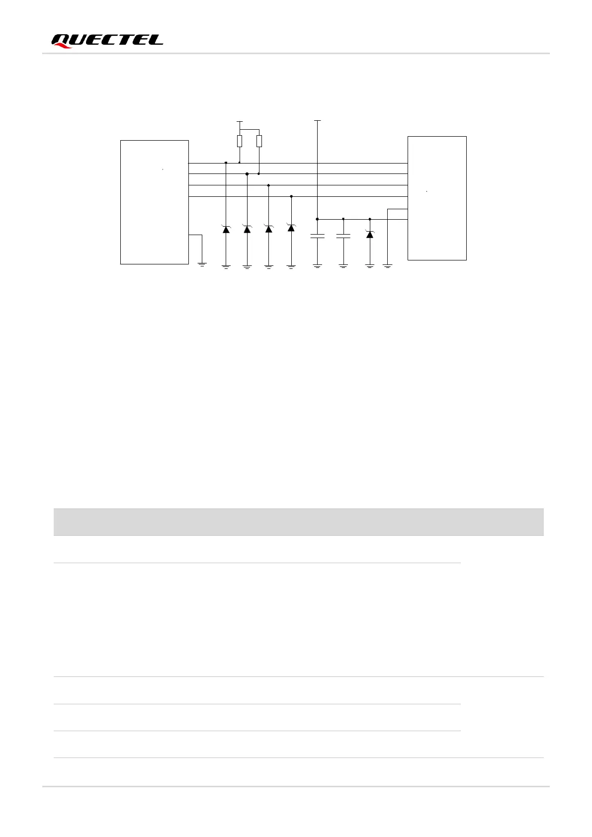
A reference design for TP interface is shown below.
TP_RST
TP_I2C_SCL
TP_I2C_SDA
TP_INT
1
2
3
4
5
6
4.7 μF
100 nF
Module
RESET 1.8 V
SCL 1.8 V
SDA 1.8 V
INT 1.8 V
GND
VDD
TP
C1 C2
D1 D2
D3
D4
D5
LDO7C_3V0
LDO18B_1V8
2.2K
R1
R2
2.2K
GND
Figure 22: Reference Circuit for TP Interface
4.13. Camera Interfaces
Based on the MIPI_CSI standard, the module provides four groups of 4-lane MIPI_CSI with maximum
transmission rate of 2.5 Gbps/lane. The module supports two cameras (4-lane + 4-lane), or three
cameras (4-lane + 4-lane + 4-lane), or four cameras (4-lane + 4-lane + 4-lane + 4-lane). The video and
photo quality are determined by various factors such as the camera sensor, camera lens quality.
Table 28: Pin Definition of Camera Interfaces
Pin Name
Pin No.
I/O
Description
Comment
VREG_L1P_1P05
116
PO
DVDD for cameras 1 and 2
When using
them, it is
recommended
to add bypass
capacitors with
a total
capacitance
not exceeding
45.3 μF.
VREG_L2P_1P1
121
PO
DVDD for cameras 0 and 3
VREG_L3P_2P8
113
PO
AVDD for cameras 1 and 3
When using
them, it is
recommended
to add bypass
capacitors with
VREG_L4P_2P9
124
PO
AVDD for camera 0
VREG_L5P_2P8
128
PO
AFVDD for camera 0

Table of Contents