RTL8169
2002/03/27 Rev.1.21
90
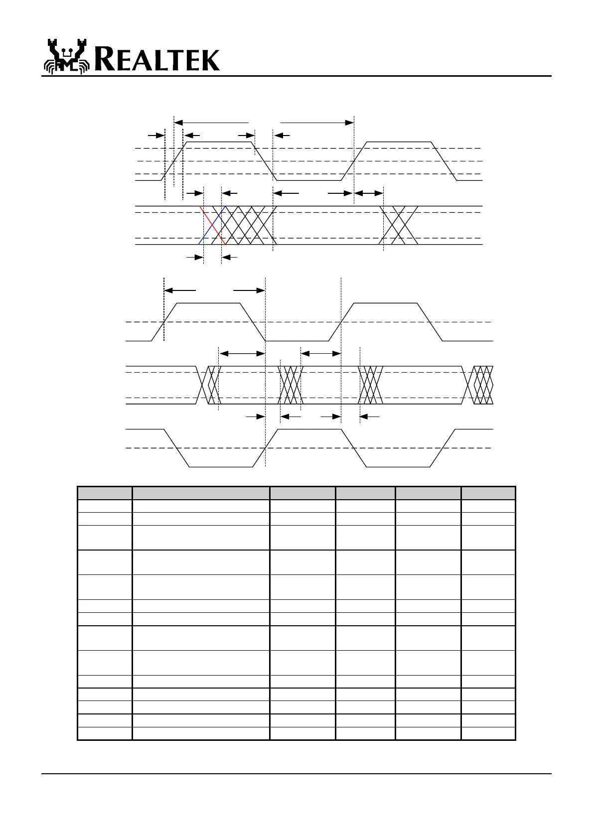
11.3.6 TBI Timing
GTxCLK
Tx[9:0]
2.0V
2.0V
0.8V
0.8V
tTxCC
tTxSU tTxHT
1.4V
Valid Data
tRC tFC
tRD
tFD
TBI Tx Timing
RxCLK0
Rx[9:0]
1.4V
2.0V
1.4V
0.8V
tA-B
tRxSU
tRxHT
RxCLK1
tRxHT
tRxSU
TBI Rx Timing
Symbol Description Min Typical Max Units
tTxCC Tx Clock Cycle 8 ns
fGTxCLK GTxCLK frequency 125 – 100ppm 125 125 + 100ppm MHz
tRC Clock Rise Time of GTxCLK,
RxCLK0, RxCLK1
0.7 2.4 ns
tFC Clock Fall Time of GTxCLK,
RxCLK0, RxCLK1
0.7 2.4 ns
tDUTY Clock Duty Cycle of GTxCLK,
RxCLK0, RxCLK1
40 60 %
tTxSU
Data Setup to ↑ of GTxCLK
2.0 ns
tTxHT
Data Hold from ↑ of GTxCLK
1.0 ns
tRD Data Rise Time of Tx[9:0],
Rx[9:0]
0.7 ns
rFD Data Fall Time of Tx[9:0],
Rx[9:0]
0.7 ns
fRxCLKx RxCLK0, RxCLK1 frequency 62.5 MHz
tDRIFT RxCLK0/1 Drift Rate 0.2 us/MHz
tRxSU
Data Setup to ↑ of RxCLK0/1
2.5 ns
tRxHT
Data Hold after ↑ of RxCLK0/1
1.5 ns
tA-B TBI RxCLK Skew 7.5 8.5 ns
TBI Timing Parameters