RL78/G13 CHAPTER 6 TIMER ARRAY UNIT
R01UH0146EJ0100 Rev.1.00 355
Sep 22, 2011
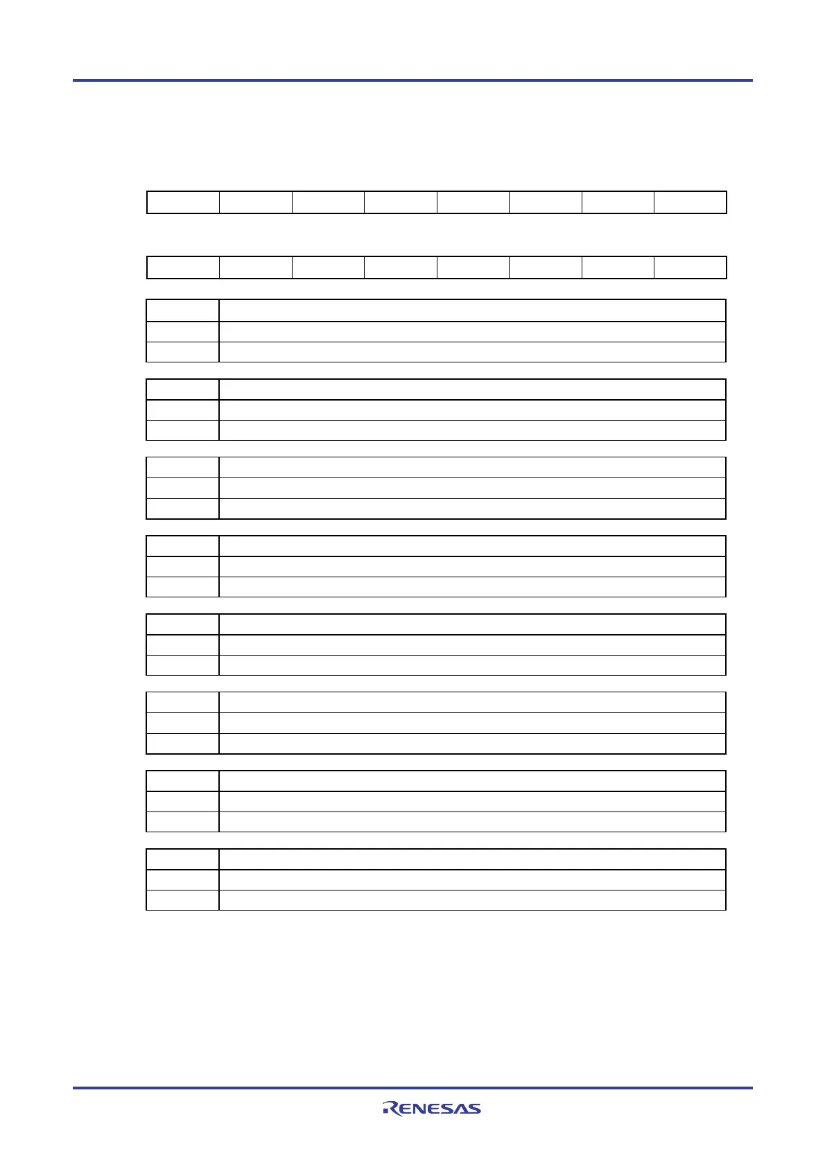
Figure 6-19. Format of Noise Filter Enable Registers 1, 2 (NFEN1, NFEN2) (1/2)
Address: F0071H After reset: 00H R/W
Symbol 7 6 5 4 3 2 1 0
NFEN1 TNFEN07 TNFEN06 TNFEN05 TNFEN04 TNFEN03 TNFEN02 TNFEN01 TNFEN00
Address: F0072H After reset: 00H R/W
Symbol 7 6 5 4 3 2 1 0
NFEN2 TNFEN17 TNFEN16 TNFEN15 TNFEN14 TNFEN13 TNFEN12 TNFEN11 TNFEN10
TNFEN07
Enable/disable using noise filter of TI07/TO07/P145 pin or RxD2/P14 pin input signal
Note
0 Noise filter OFF
1 Noise filter ON
TNFEN06 Enable/disable using noise filter of TI06/TO06/P102 pin input signal
0 Noise filter OFF
1 Noise filter ON
TNFEN05 Enable/disable using noise filter of TI05/TO05/P46 pin input signal
0 Noise filter OFF
1 Noise filter ON
TNFEN04 Enable/disable using noise filter of TI04/TO04/P04 pin input signal
0 Noise filter OFF
1 Noise filter ON
TNFEN03 Enable/disable using noise filter of TI03/TO03/P31 pin input signal
0 Noise filter OFF
1 Noise filter ON
TNFEN02 Enable/disable using noise filter of TI02/TO02/P17 pin input signal
0 Noise filter OFF
1 Noise filter ON
TNFEN01 Enable/disable using noise filter of TI01/P01/P16 pin input signal
0 Noise filter OFF
1 Noise filter ON
TNFEN00 Enable/disable using noise filter of TI00/P00 pin input signal
0 Noise filter OFF
1 Noise filter ON
Note The applicable pin can be switched by setting the ISC1 bit of the ISC register.
ISC1 = 0: Whether or not to use the noise filter of the TI07 pin can be selected.
ISC1 = 1: Whether or not to use the noise filter of the RxD2 pin can be selected.
Remark The presence or absence of timer I/O pins of channel 0 to 7 depends on the product. See Table 6-2
Timer I/O Pins provided in Each Product for details.

 Loading...


