EasyManuals Logo
Home>Renesas>Computer Hardware>RZ Series

Renesas RZ Series User Manual

Renesas RZ Series
83 pages
To Next Page IconTo Next Page
To Previous Page IconTo Previous Page
Page #43 background imageLoading...
Page #43 background image
RZ/G, RZ/V
Series
RZ Family / RZ/G, RZ/A Series 2. Functional Specifications
R01UH0990EJ0101 Rev.1.01 Page 43 of 83
Jul 28, 2022
2.3 Memory
QSPI flash memory and DDR4 SDRAM are mounted on the RTK9743U11C01000BE as external memories.
Please refer to the following for details.
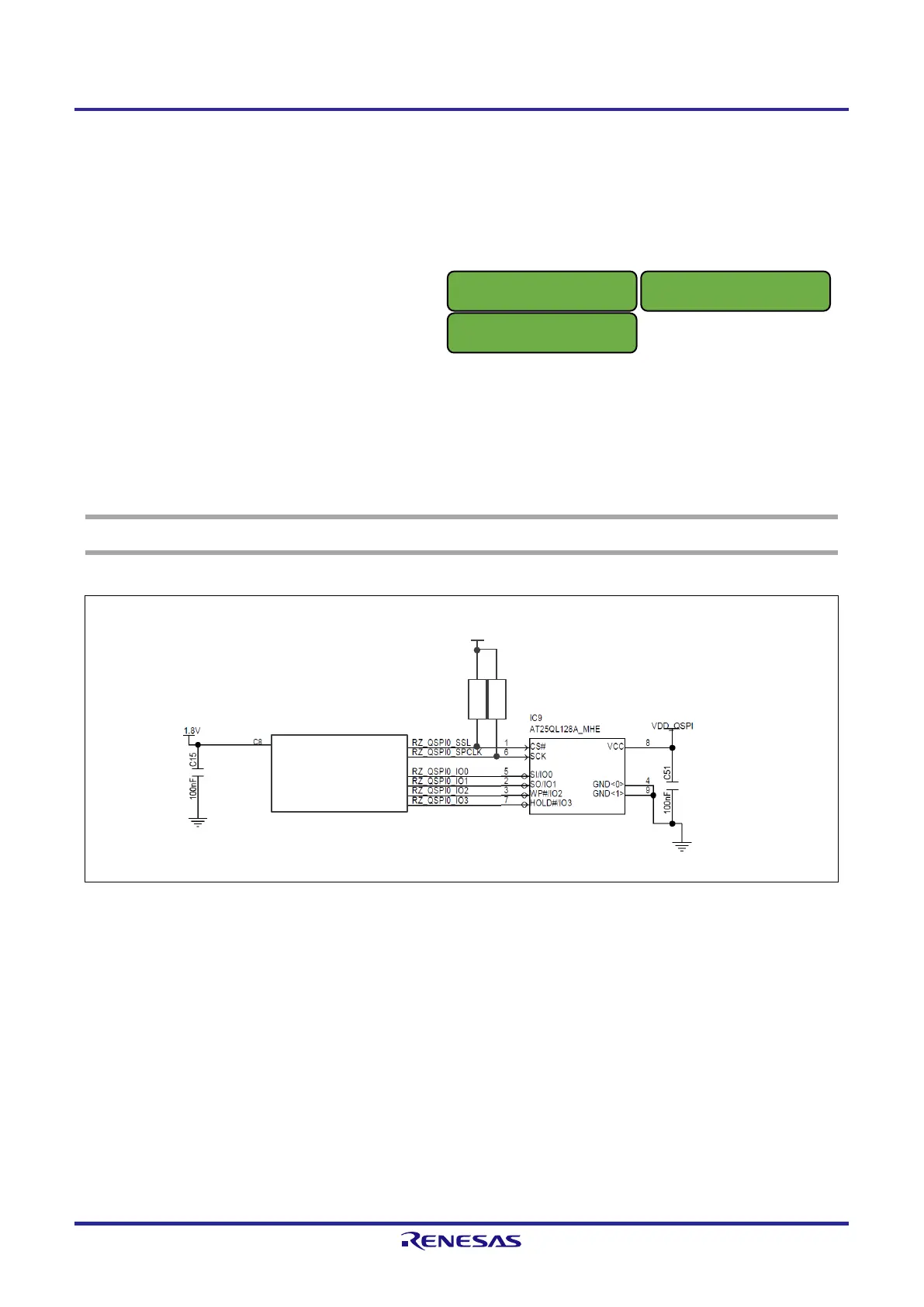
2.3.1 QSPI Flash Memory
Figure 2.1 shows a block diagram of the Serial Flash Memory Interface.
The QSPI flash memory is controlled by the SPI Multi I/O Bus Controller (SPIBSC) that is with built-in to the
RZ/G2UL. This memory supports both single data rate (SDR) and double data rate (DDR) transfers at 66 MHz and 50
MHz clock frequency.
NOTE
The pull-up resistor on the clock line “RZ_QSPI0_SPCLK” is optional.
Figure 2.1 Block Diagram of Serial Flash Memory I/F
SPI_PVDD QSPI0_SSL
QSPI0_SPCLK
QSPI0_IO0
QSPI0_IO1
QSPI0_IO2
QSPI0_IO3
RZ/G2UL, RZ/A3UL, RZ/Five
10k
10k
1.8V
R57
R22
RZ/A3UL SMARC Module Board
QSPI Edition
RZ/G2UL SMARC Module Board
RZ/Five SMARC Module Board

Table of Contents

Other manuals for Renesas RZ Series

Questions and Answers:

Question and Answer IconNeed help?

Do you have a question about the Renesas RZ Series and is the answer not in the manual?

Renesas RZ Series Specifications

General IconGeneral
BrandRenesas
ModelRZ Series
CategoryComputer Hardware
LanguageEnglish

Related product manuals