RZ Family / RZ/G, RZ/A Series 2. Functional Specifications
R01UH0990EJ0101 Rev.1.01 Page 54 of 83
Jul 28, 2022
2.10 Debug Interface
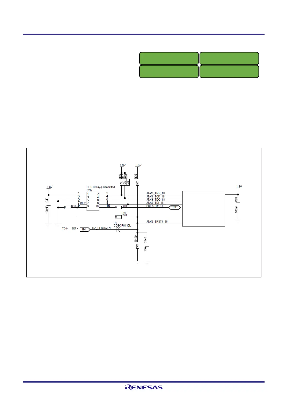
Figure 2.12 shows a block diagram of debug interface.
Ths interface supports JTAG and SWD and has debug support for Cortex-A55 and Cortex-M33.
The default operation for the debug interface uses pin 9 as a ground detect, although with resitor(R20) fitting options, it
is possible to use this to independently drive the JTAG_TRST#.
When debug mode is disabled (SW1-1: DEBUGEN is ON), JTAG_TRST# is permanently low.
On the other hands, when debug mode is enabled (SW1-1: DEBUGEN is OFF), JTAG_TRST# is initially low on
powerup and then ramps up to 1.8V.
Figure 2.12 Block Diagram of Debug I/F
 Loading...


