Chapter 3 – SD Card Interface Description
Revision 2.2 SD Card Product Manual
© 2004 SanDisk Corporation 3-18 12/08/04
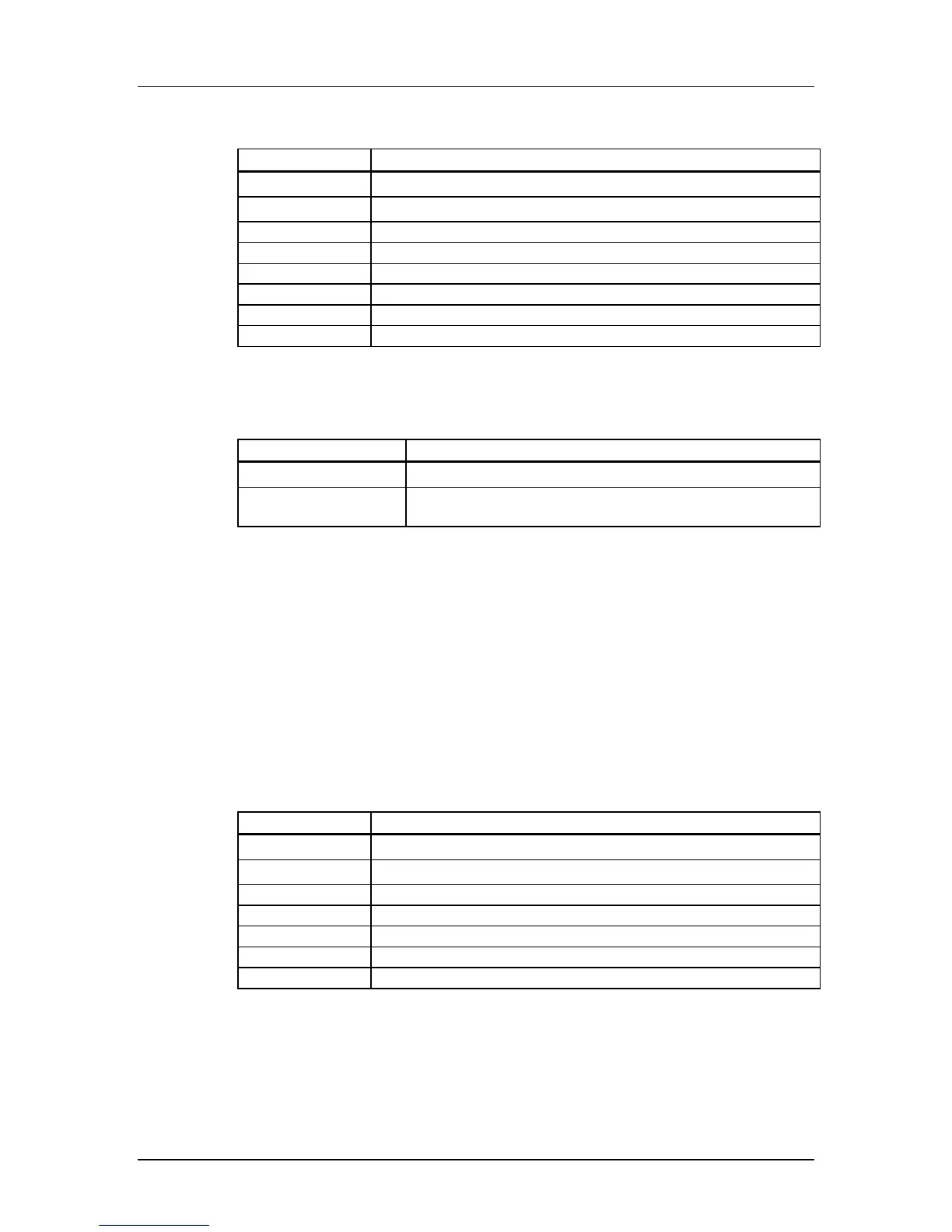
Table 3-23 Device Size Multiplying Factor
C_SIZE_MULT MULT
0 2
2
= 4
1 2
3
= 8
2 2
4
= 16
3 2
5
= 32
4 2
6
= 64
5 2
7
= 128
6 2
8
= 256
7 2
9
= 512
• ERASE_BLK_EN— determines whether erasing one write block (see
WRITE_BL_LEN) is allowed (other than SECTOR_SIZE given below).
Table 3-24 Bit Definition
ERASE_BLK_EN Definition
0 Host can erase a SECTOR_SIZE unit.
1 Host can erase either a SECTOR_SIZE unit or a WRITE_BLK_LEN
unit.
• SECTOR_SIZE—contents of this register is a 7-bit binary-coded value, defining the
number of write blocks (see WRITE_BL_LEN). The actual size is computed by
increasing this number by one. A value of “0” denotes 1 write block, 127 denotes 128
blocks.
• WP_GRP_SIZE—contents of this register is a 5-bit binary-coded value, defining the
number of Erase Groups (see SECTOR_SIZE). The actual size is computed by
increasing this number by “1”. A value of “0” denotes 1 erase group, and a value of
“127” denotes 128 erase groups.
• WP_GRP_ENABLE—A value of “0” means group write protection is not possible.
• R2W_FACTOR—defines the typical block program time as a multiple of the read
access time. Table 3-25 defines the field format.
Table 3-25 R2W_FACTOR
R2W_FACTOR Multiples of Read Access Time
0 1
1 2 (write half as fast as read)
2 4
3 8
4 16
5 32
6, 7 Reserved
• WRITE_BL_LEN— The maximum write data block length is computed as
2
WRITE_BL_LEN
. The maximum block length might therefore be in the range 512…2048
bytes. A 512-byte write block length is always supported. In the SD Memory Card,
the WRITE_BL_LEN is always equal to READ_BL_LEN.
 Loading...