LC-32/40/46LE700E/RU/S,LU700E/S,LX700E/RU,LC-52LE700E/RU/S
7 – 16
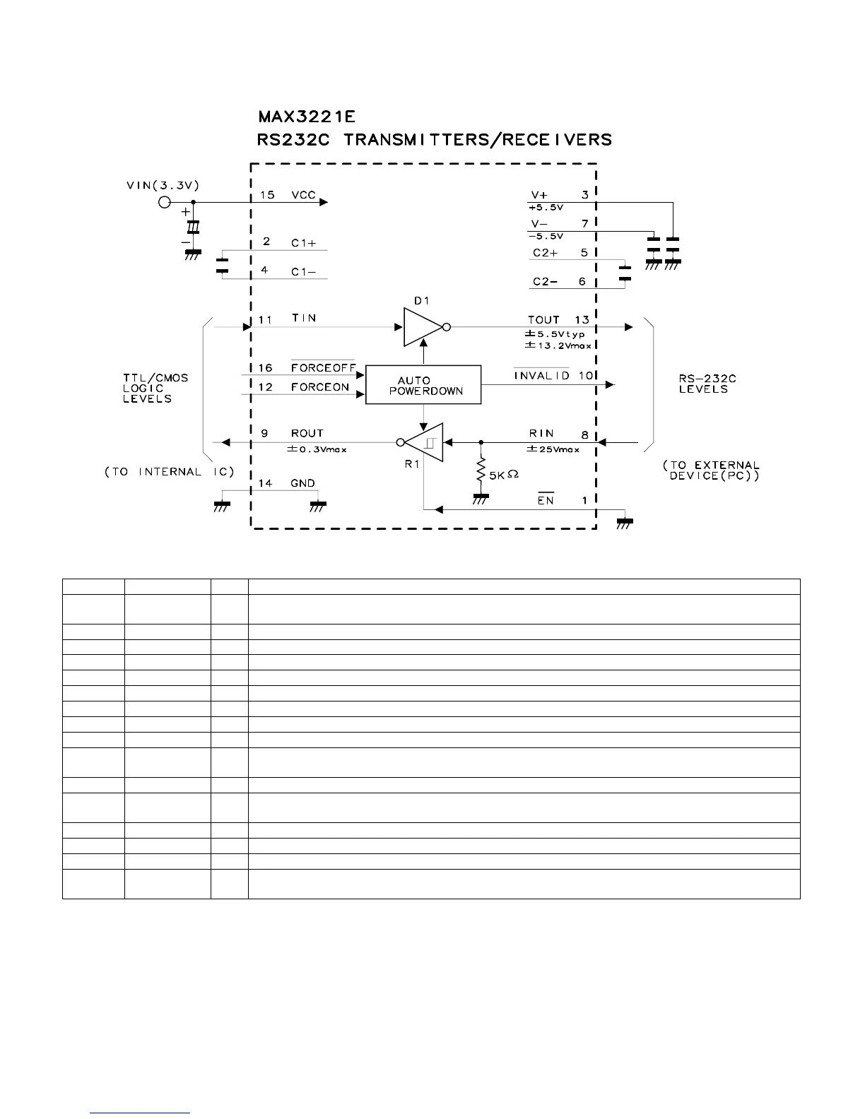
2.11. IC506 (VHiM3221EiP-1Y)
2.11.1 Block Diagram
2.11.2 Pin Connections and short description
Pin No. Pin Name I/O Pin Function
1EN I
Receiver Enable Control . Drive low for normal operation. Drive high to force the receiver outputs (R_OUT)
into a high-impedance state.
2 C1+ - Positive terminal of the voltage doubler Charge-Pump Capacitor
3 V+ - +5.5V generated by the charge pump
4 C1- - Negative terminal of the voltage doubler Charge-Pump Capacitor
5 C2+ - Positive terminal of inverting Charge-Pump Capacitor
6 C2- - Negative terminal of inverting Charge-Pump Capacitor
7 V- - -5.5V generated by the charge pump
8 R_IN I RS-232 Receiver Inputs
9 R_OUT O TTL/CMOS Receiver Outputs
10 INVALID I
Output of the Valid Signal Detector. INVALID is enabled high if a valid RS-232 level is present on any receiver
input.
11 T_IN I TTL/CMOS Transmitter Inputs
12 FORCEON I
Drive high to override automatic circuitry keeping transmitters and charge pump on (FORCEOFF must be
high)
13 T_OUT O RS-232 Transmitter Outputs
14 GND - Ground
15 VCC - +3.0V to +5.5V Supply Voltage
16 FORCEOFF I
Force-Off Input, active low. Drive low to shut down transmitters, receivers (MAX3243E, except R2OUTB),
and on-board charge pump . This overrides all automatic circuitry and FORCE ON