LC-52XS1E/RU/LC-65XS1E/RU
5 – 4
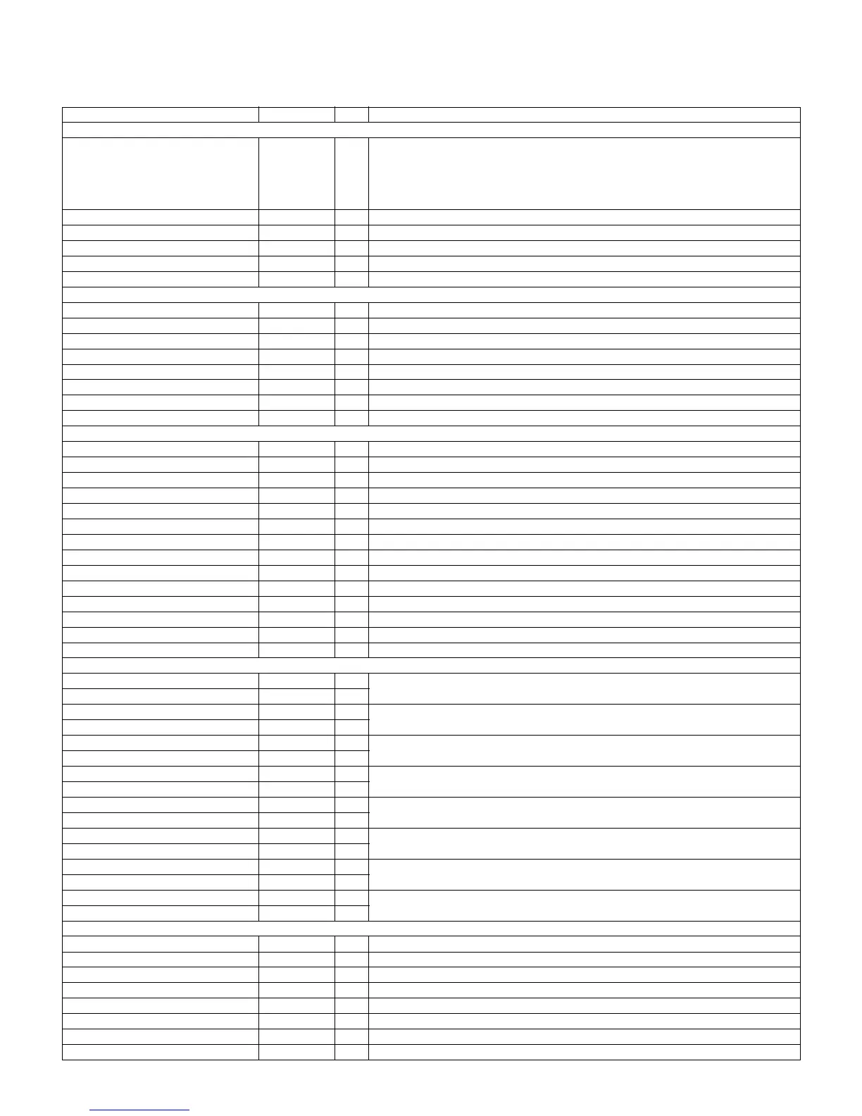
3. IC6102 (VHiSii9125+-1Q)
This is an HDMI Rx, which converts the differential signals input from IC6004 into 8-bit RGBs of LVTTL.
HDMI Receiver
Pin No. Pin Name I/O Pin Function
Digital Video Output Pins.
16, 15, 14, 13, 10, 9, 8, 7, 3, 2, 1,
144, 141, 140, 139, 138, 135, 134,
133, 132, 129, 128, 127, 126, 123,
122, 121, 120, 117, 116, 115, 114,
111, 110, 109, 108
Q[35:0] O
36-bit Output Pixel Data Bus.
Q[35:0] is highly configurable using the VDD_CONFIG resister.
It supports a wide array of output formats, including multiple RGB and YCbCr bus for-
mats.
19 DE O Data enable.
20 HSYNC O Horizontal Sync Output control signal.
21 VSYNC O Vertical Sync Output control signal.
22 EVNODD O indicates Even or Odd Field for interlaced Formats.
5 ODCK O Output Data Clock.
Digital Audio Output Pins.
95 XTALIN I Crystal Clock Input. 26-28.5MHz
94 XTALOUT O Crystal Clock Output.
89 MCLK O Audio Master Clock Output.
86 SCK O I2S Serial Clock Output.
85 WS O I2S Word Select Output.
81 SD O I2S Serial Data Output.
78 SPDIF O S/PDIF Audio Output.
75 MUTEOUT O Mute Audio Output.
Configuration/Programming Pins.
102 INT O Interrupt Output.
100 RESET# I Reset Pin. Active LOW. 5V Tolerant.
34 DSCL0 I DDCI2C Clock for Port 0. 5V Tolerant.
33 DSDA0 I/O DDCI2C Data for Port 0. 5V Tolerant.
29 DSCL1 I DDCI2C Clock for Port 1. 5V Tolerant.
28 DSDA1 I/O DDCI2C Data for Port 1. 5V Tolerant.
27 CSCL I Configuration/Status I2C Clock. 5V Tolerant.
26 CSDA I/O Configuration/Status I2C Data. 5V Tolerant.
105 CI2CA I Local I2C Address Select. 5V Tolerant.
101 SCDT O Indicates active video at HDMI input port.
35 R0PWR5V I Port 0 Transmitter Detect. 5V Tolerant.
30 R1PWR5V I Port 1 Transmitter Detect. 5V Tolerant.
98,77,76,55,82,83,84 RSVDNC - Reserved, must be left unconnected.
99 RSVDL I Reserved, must be tied to ground.
Differential Signal Data Pins.
40 R0XC+ I
TMDS input clock pair. HDMI Port 0.
39 R0XC- I
44 R0X0+ I
TMDS input data pair. HDMI Port 0.
43 R0X0- I
48 R0X1+ I
TMDS input data pair. HDMI Port 0.
47 R0X1- I
52 R0X2+ I
TMDS input data pair. HDMI Port 0.
51 R0X2- I
58 R1XC+ I
TMDS input clock pair. HDMI Port 1.
57 R1XC- I
62 R1X0+ I
TMDS input data pair. HDMI Port 1.
61 R1X0- I
66 R1X1+ I
TMDS input data pair. HDMI Port 1.
65 R1X1- I
70 R1X2+ I
TMDS input data pair. HDMI Port 1.
69 R1X2- I
Power and Ground Pins.
12, 24, 25, 80, 91, 107, 119, 131, 143 CVCC18 --- Digital Logic VCC. 1.8V
11, 23, 79, 90, 106, 118, 130, 142 CGND --- Digital Logic ground.
6, 18, 32, 74, 88, 104, 113, 125, 137 IOVCC33 --- Input/Output Pin Supply. 3.3V
4, 17, 31, 73, 87, 103, 112, 124, 136 IOGND --- Input/Output Pin ground.
38, 42, 46, 50, 56, 60, 64, 68 AVCC33 --- TMDS Analog VCC. 3.3V
36, 41, 45, 49, 53, 59, 63, 67, 71 AGND --- TMDS Analog ground.
37,54,72 AVCC18 --- TMDS Analog VCC 1.8V.
92 DVCC18 --- Audio clock regeneration PLL analog VCC. 1.8V
 Loading...