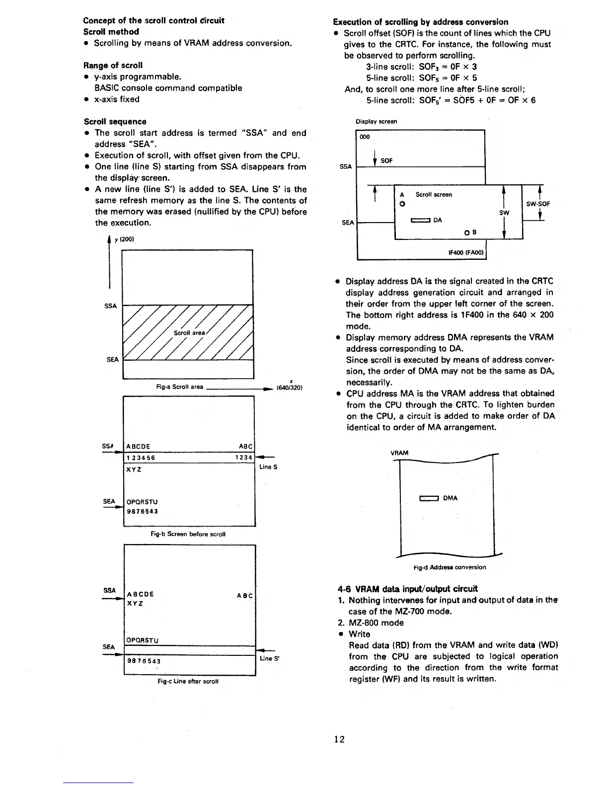
Concept of
the
.scroll
control
C!ircuit
Scroll
method
• Scrolling
by
means
of
VRAM address conversion.
Range of scroll
• y-axis programmable.
BASIC
console command compatible
• x-axis fixed
Scroll
sequence
• The scroll start address is termed
"SSA"
and end
address
"SEA".
• Execution
of
scroll,
with
offset given
from
the
CPU.
• One line (line
S)
starting
from
SSA disappears from
the
display· screen.
• A new line (line S') is added
to
SEA. Line S' is the
same refresh
memory
as
the line
S.
The contents
of
the
memory
was erased (nullified by the
CPU)
before
the execution.
SSP
SEA
---
SSA
~
SEA
X
Rg-a Scroll area
------•
(6401320}
A
BC
DE
ABC
1
23456
1234
1----
XYZ
Line
s
OPQRSTU
9876543
Fig-b Screen before scroll
ABCDE
ABC
XYZ
OPQRSTU
r--
9876543
Line
s·
Fig-c Line after scroll
Execution of scrolling by
address
conversion
• Scroll offset
(SOF)
is the count
of
lines which the
CPU
gives to the
CRTC.
For instance, the following must
be
observed to perform scrolling.
3-line scroll:
SOF
3
=
OF
x 3
5-line scroll:
SOF
5
=OF
x 5
And, to
scroll one more line after 5-line scroll;
5-line scroll:
SOF
5
'
=
SOF5
+OF=
OF
x 6
Display screen
000
SOF
SSA
t----'-----------1
A Scroll screen
0
SEA~---1
t:::=::l
DA
OB
IF400
(FAOO}
• Display address DA
is
the signal created in the
CRTC
display address generation circuit and arranged in
their order from the upper
left corner
of
the screen.
The
bottom
right address is 1
F400
in the 640 x
200
mode.
• Display
memory
address DMA represents the VRAM
address corresponding
to
DA.
Since
scroll is executed by means
of
address conver-
sion, the order
of
DMA may not
be
the same
as
DA,
necessarily.
•
CPU
address
MA
is the VRAM address that obtained
from
the
CPU
through the
CRTC.
To lighten burden
on the
CPU,
a circuit is added to make order
of
DA
identical to order
of
MA
arrangement.
VRAM
Fig-d Address conversion
4-6
VRAM
data input/output circuit
1.
Nothing intervenes
for
input
and
output
of
data in the
case
of
the MZ-700 mode.
2.
MZ-800
mode
• Write
12
Read data
(RD)
from
the VRAM and write data
(WO)
from
the
CPU
are subjected
to
logical operation
according
to
the direction
from
the write format
register
(WF)
and its result is written.
 Loading...