Parameter list
7.2 Parameter list
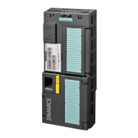
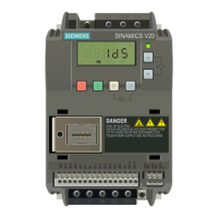
SINAMICS V20 Inverter
214 Operating Instructions, 07/2012, A5E03728167
Parameter Function Range Factory
default
Can be
changed
Scaling Data
set
Data
type
Acc.
Level
[12] Enable CMP 1
[13] Enable CMP 2
Dependency: Set P2800 to 1 to enable function blocks.
All active function blocks, enabled with P2802, will be calculated in every 128 ms.
P2803[0...2] Enable Fast FFBs 0 - 1 0 U, T - CDS U16 3
Fast free function blocks (FFB) are enabled in two steps:
1. P2803 enables the use of fast free function blocks (P2803 = 1).
2. P2801 enables each fast free function block individually and determines the chronological order
(P2801[x] = 4 ... 6).
0 Disable
1 Enable
Dependency: All active fast function blocks will be calculated in every 8 ms.
Note: Attention: P2200 and P2803 are locked parameter against each other. PID and FFB of the same data set
cannot be active at same time.
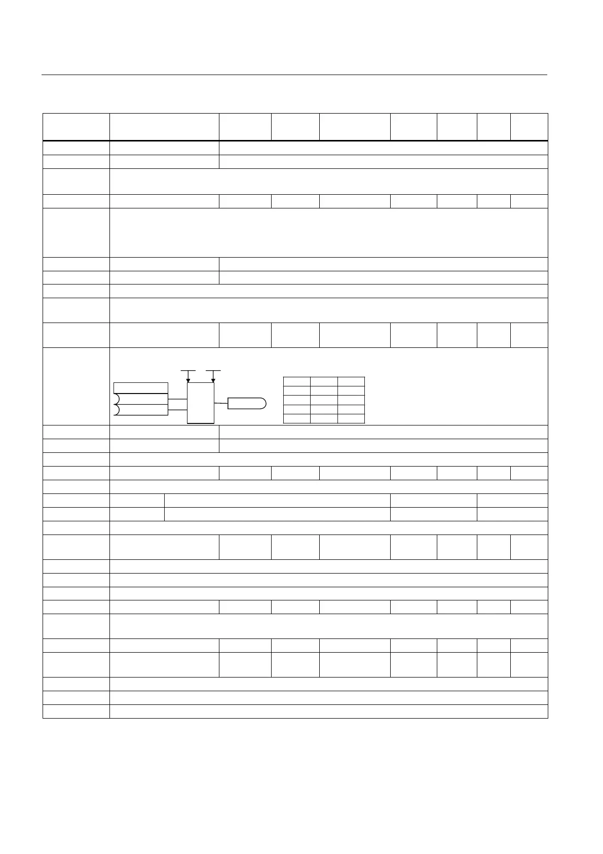
P2810[0...1] BI: AND 1 - 0 U, T - - U32 /
Bin
3
P2810[0], P2810[1] define inputs of AND 1 element, output is r2811.
P2800 P2801[0]
A
B
C
&
P2810
r2811
ABC
000
010
100
111
,QGH[
,QGH[
Index: [0] Binector input 0 (BI 0)
[1] Binector input 1 (BI 1)
Dependency: P2801[0] assigns the AND element to the processing sequence.
r2811.0 BO: AND 1 - - - - - U16 3
Output of AND 1 element. Displays and logic of bits defined in P2810[0], P2810[1].
Bit Signal name 1 signal 0 signal
00 Output of BO Yes No
Dependency: See P2810
P2812[0...1] BI: AND 2 - 0 U, T - - U32 /
Bin
3
P2812[0], 2812[1] define inputs of AND 2 element, output is r2813.
Index: See P2810
Dependency: P2801[1] assigns the AND element to the processing sequence.
r2813.0 BO: AND 2 - - - - - U16 3
Output of AND 2 element. Displays and logic of bits defined in P2812[0], P2812[1]. See r2811 for the bit
field description.
Dependency: See P2812
P2814[0...1] BI: AND 3 - 0 U, T - - U32 /
Bin
3
P2814[0], P2814[1] define inputs of AND 3 element, output is r2815.
Index: See P2810
Dependency: P2801[2] assigns the AND element to the processing sequence.
 Loading...