3.1 Mounting and Connections
355
7UT613/63x Manual
C53000-G1176-C160-2
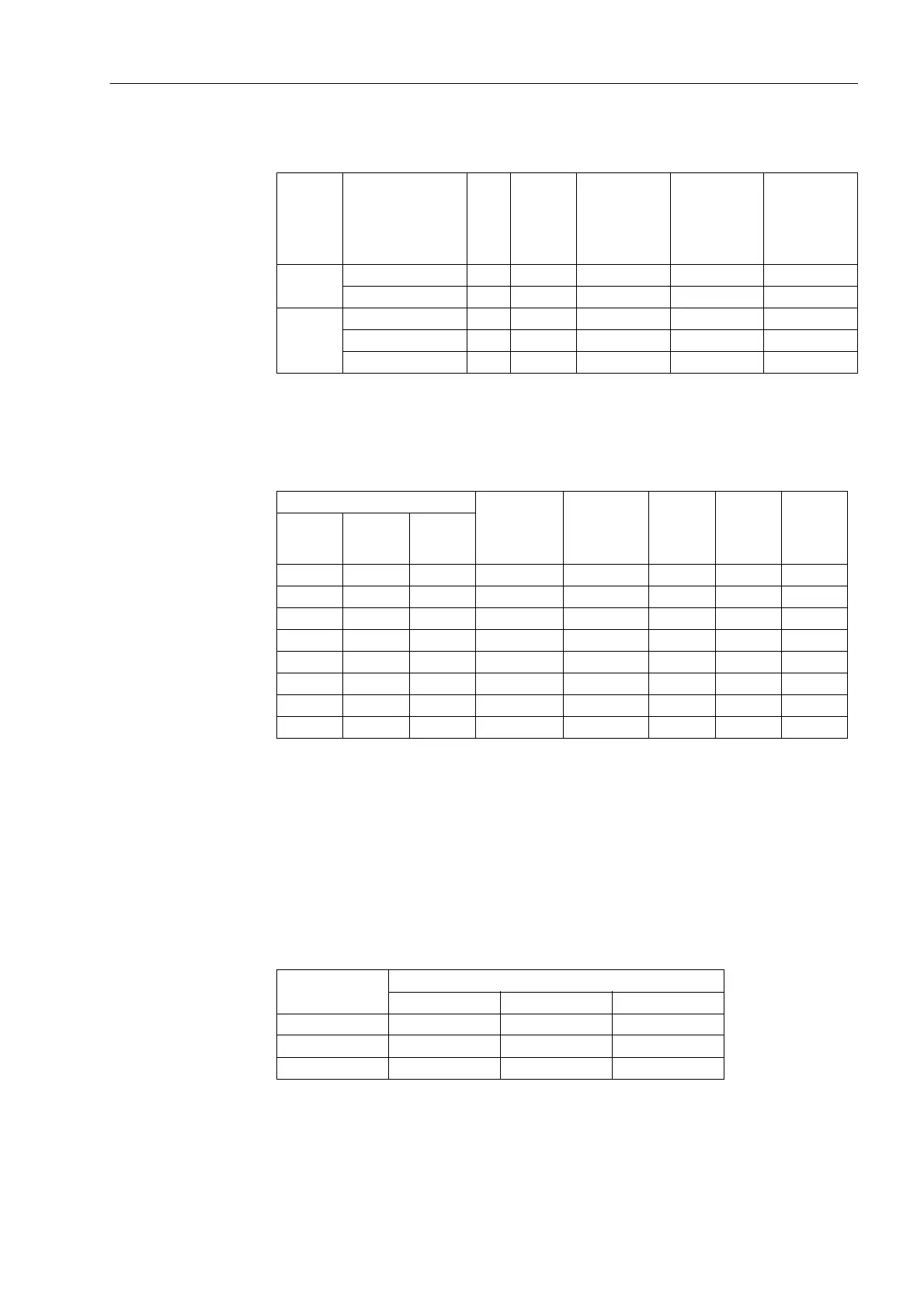
Table 3-8 Jumper settings of the contact type of relays of the binary outputs BO1, BO9
and BO17 on the input/output boards C-I/O-1
The pickup voltages of the binary inputs BI6 through BI29 are checked according to
the following table
Table 3-9 Jumper settings of the pickup voltages of the binary inputs BI6 through BI29
on the input/output board C-I/O-1 or C-I/O-10
1)
Only for C-I/O-1
2)
Factory settings for devices with power supply voltages 24 VDC to 125 VDC
3)
Factory settings for devices with power supply voltages of 110 VDC to 250 VDC and 115 VAC
4)
Factory settings for devices with power supply voltages of 220 VDC to 250 VDC and 115 VAC
The jumpers X71 through X73 serve for setting the bus address. Their position may
not be changed. The following tables list the jumper presettings.
Table 3-10 Jumper settings of the module addresses of the input/output boards C-I/O-1
and C-I/O-10
Device Module For Jumper
Quiescent
State
open
(close)
Quiescent
State
closed
(open)
Default Posi-
tion
7UT633
Slot 33 left side BO9 X40 1-2 2-3 1-2
Slot 19 left side BO17 X40 1-2 2-3 1-2
7UT635
Slot 5 right side BO1 X40 1-2 2-3 1-2
Slot 33 left side BO9 X40 1-2 2-3 1-2
Slot 19 left side BO17 X40 1-2 2-3 1-2
Binary inputs Jumpers on
C-I/O-1 and
C-I/O-10
Jumpers on
C-I/O-10 up
release EE
or higher
Thres-
hold 17
V
2
)
Thres-
hold 73
V
3
)
Thres-
hold 154
V
4
)
Slot 33
left side
Slot 19
left
1
)
Slot 5
right
1
)
BI6 BI14 BI22 X21/X22 X21 L M H
BI7 BI15 BI23 X23/X24 X23 L M H
BI8 BI16 BI24 X25/X26 X25 L M H
BI9 BI17 BI25 X27/X28 X27 L M H
BI10 BI18 BI26 X29/X30 X29 L M H
BI11 BI19 BI27 X31/X32 X31 L M H
BI12 BI20 BI28 X33/X34 X33 L M H
BI13 BI21 BI29 X35/X36 X35 L M H
Jumper
Mounting Location
Slot 19 left side Slot 33 left side Slot 5 right side
X71 H L H
X72 L H H
X73 H L H
 Loading...