Smart Machine Smart Decision
SIM868_Series_Hardware_Design_V1.06 25 2017-07-13
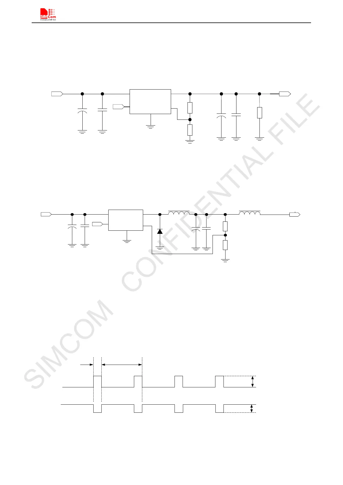
5.2. Reference Circuit of GSM Power Supply
Figure 10 is the reference design of +5V input power supply. The output power supply is 4.1V, thus a linear
regulator can be used.
Vin
Vout
GND
FB
3
+
PWR_CTRL
R102
R101
GSM_VBAT
100K
43K
+
C103
330uF
C104
100nF
U101
MIC29302
5
4
1
2
C101 C102
100uF
1uF
DC INPUT
R103
470Ω
On/Off
Figure 10: Reference circuit of the LDO power supply
If there is a high drop-out between the input and the desired output (GSM_VBAT), a DC-DC power supply will
be preferable because of its better efficiency especially with the 2A peak current in burst mode of the GSM.
Figure 11is the reference circuit.
Vin
Vout
FB
U101
1
2
3
4
5
LM2596- ADJ
+
100uH
MBR360
L101
C101
+
C102
D10
2
C103
R102
R101
FB101
330uF
GSM_VBAT
2.2K
1K
100uF
1uF
C104
100nF
270
DC input
PWR_CTR
L
GND
Ω
On/Off
Figure 11: Reference circuit of the DC-DC power supply
When battery is used, the total impedance between battery and GSM_VBAT pins should be less than 150mΩ.
Figure 12 shows the GSM_VBAT voltage drop at the maximum power transmit phase, and the test condition is
as following:
GSM_VBAT=4.0V,
A GSM_VBAT bypass capacitor C
A
=100µF tantalum capacitor (ESR=0.7Ω),
Another GSM_VBAT bypass capacitor C
B
=1uF~10uF.
577us 4.615ms
Burst:2A
I
GSM_VBAT
GSM_VBAT
Max:350mV
Figure 12: The minimal VBAT voltage requirement at VBAT drop