Smart Machine Smart Decision
SIM868_Series_Hardware_Design_V1.06 32 2017-07-13
VDD_EXT
4.7K
47K
UART1_TXD
4.7K
GSM
VDD_EXT
RXD
VDD
DTE
Figure 21: TX level matching circuit
VDD_EXT
4.7K
47K
4.7K
DTE
UART1_RXD
GSM
VDD_EXT
TXD
VDD
Figure 22: RX level matching circuit
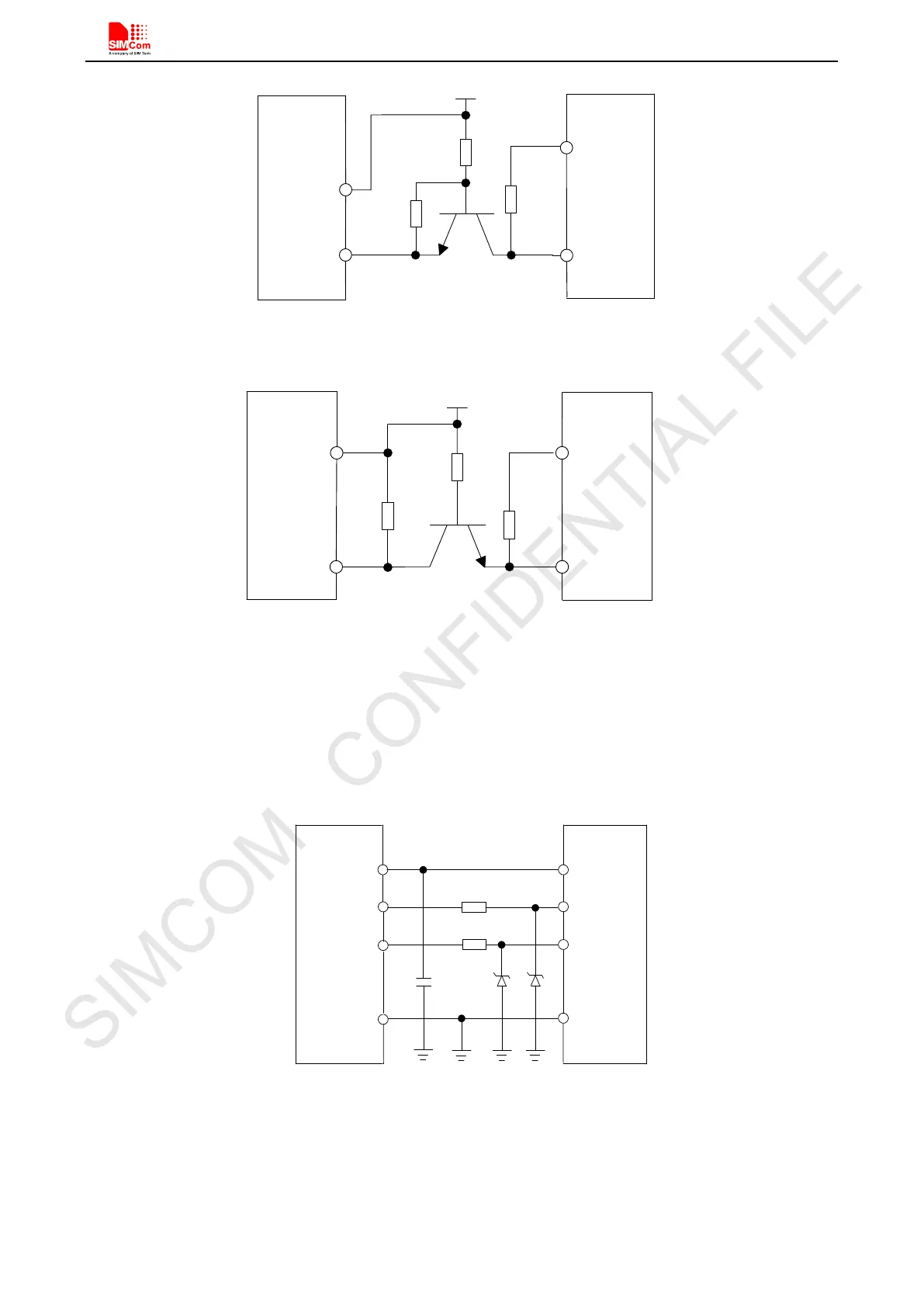
5.5.3. Debug Interface
GSM could be debugged through USB port. The recommended diagram is shown as Figure 23:
GSM
USB
GND
GND
22R
USB_VBUS
VBUS
1uF
USB_DM
USB_DP
USB_DM
22R
USB_DP
Figure 23: USB reference circuit
The TVS on USB data line should be less than 5pF, and the USB signals have to be layout according to
differential signal layout rules.
Note: Please reserve the USB interface or test point for further debugging.