Smart Machine Smart Decision
SIM868_Series_Hardware_Design_V1.06 56 2017-07-13
7. PCB Layout
This section provides some guidelines on PCB layout, in order to eliminate interference or noise.
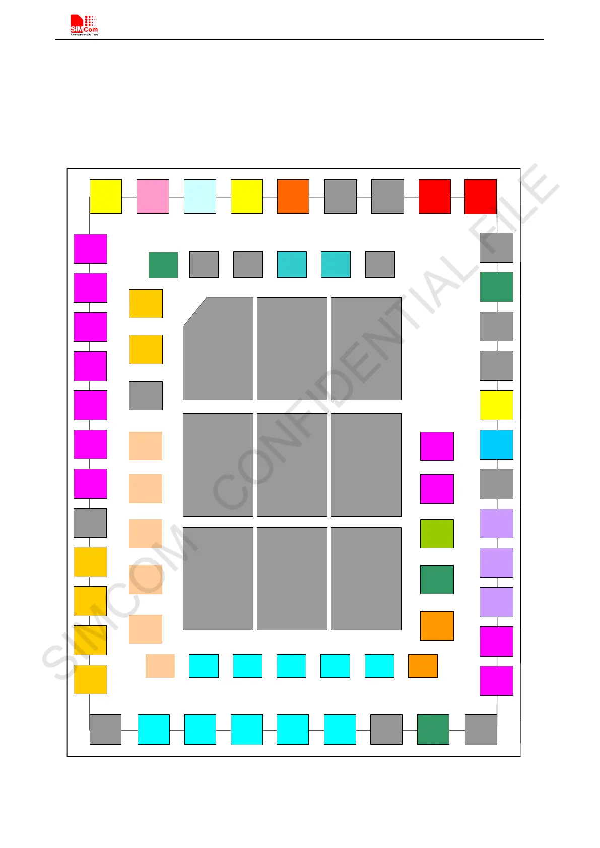
7.1. Pin Assignment
Before PCB layout, we should learn about pin assignment in order to get reasonable layout with so many
external components. Figure 51 is the overview of pin assignment of the module.
MCCK
UART1_DTR
USB_DP
GPS_VBAT
VBAT
ADC
UART1_RXD
PWRKEY
UART1_CTS
UART1_TXD
UART1_RTS
SCL SDA
UART1_DCD
NETLIGHT
SIM1_RSTSIM1_CLK
SIM1_DET
SIM1_DATA
BT_ANT
SIM2_CLKSIM2_DET SIM2_DATA
SIM2_RST
SIM
2_VDD
UART2_TXD
SPK1P
VRTC
MICP
MICN
USB_VBUS
USB_DM
GSM_ANT
STATUS
SIM1_VDD
MCCA3
GND
UART2_RXD
GND
GPS_RXD
GNSS_EN
1
PPS
GPIO2
GPS_TXD
13
SPK1N
UART1_RI
GPS_ANT
14 15 16 2117 18 19 20
22
23
24
25
26
27
28
29
30
31
32
33
37
36 35
34
1
42
41
40
39
38
5
4
2
3
6
11
10
9
8
7
51
12
5352 55
54
57
56
58
62
61
60
59
67 66 65 64 63
46
45
44
43
49
48
47
50
VDD_EXT
GND
GND
GND
GND
GND
GND
GPIO1
GND
GND
GND
GND
UART1_DTR
RF_SYNC
GND
GND
SPK2P
68
MCCM0
MCCA1
SPK2N
MCCA2
MCCA0
GND
GNDGND
GNDGNDGND
GND
GNDGND
7669
75
70 77 74
71 72
73
Figure 51: PIN assignment