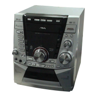
CX-BK1
3
TABLE OF CONTENTS
1. SERVICING NOTES ................................................ 4
2. GENERAL
Location of Controls ....................................................... 6
3. DISASSEMBLY
3-1. Disassembly Flow ........................................................... 8
3-2. Panel ................................................................................ 9
3-3. Top Panel Block .............................................................. 9
3-4. Front Panel Assy ............................................................. 10
3-5. MAIN Board ................................................................... 10
3-6. Rear Cover....................................................................... 11
3-7. Tuner (FM/AM) .............................................................. 11
3-8. SPEAKER Board ............................................................ 12
3-9. ACDC Board, Power Transformer.................................. 12
3-10. AMP Board ..................................................................... 13
3-11. CD Mechanism Deck (CDM69BV-30CBD64NS)......... 13
3-12. Signal Cassette Mechanism ............................................ 14
3-13. Base Unit Section............................................................ 14
3-14. Base Unit (BU-30CBD64NS)......................................... 15
3-15. BD Board......................................................................... 15
3-16. SW (1) Board, SW (2) Board, SW (3) Board,
SW (4) Board, Bracket (Top) Assy................................. 16
3-17. CONNECTOR Board ..................................................... 16
3-18. Motor (Stocker) Assy (Stocker) (M761) ........................ 17
3-19. Motor (Roller) Assy (Roller) (M781)............................. 17
3-20. Motor (Mode) Assy (Mode) (M771) .............................. 18
3-21. Rubber Roller (Slider) Assy ........................................... 18
3-22. Timing Belt (Front/Rear) ................................................ 19
3-23. Cam (Gear) ...................................................................... 19
3-24. SENSOR Board............................................................... 20
4. ASSEMBLY
4-1. How to Install the Cam (Eject Lock).............................. 21
4-2. How to Install the Cam (Gear)........................................ 21
4-3. How to Install the Gear (Mode C) .................................. 22
4-4. How to Install the Gear (Mode Cam) ............................. 22
4-5. How to Install the Rotary Encoder (S702),
Gear (Stocker Communication) ...................................... 23
4-6. How to Install the Stocker Assy...................................... 23
5. TEST MODE.............................................................. 24
6. MECHANICAL ADJUSTMENTS ....................... 25
7. ELECTRICAL ADJUSTMENTS
Deck Section ................................................................... 25
CD Section ...................................................................... 28
8. DIAGRAMS
8-1. Block Diagram – CD Section – ..................................... 31
8-2. Block Diagram – TUNER/TAPE/USB Section – ......... 32
8-3. Block Diagram – AMP Section – .................................. 33
8-4. Block Diagram – POWER SUPPLY Section – ............. 34
8-5. Note for Printed Wiring Boards
and Schematic Diagrams ................................................ 35
8-6. Printed Wiring Board – BD Board – ............................. 36
8-7. Schematic Diagram – BD Board – ................................ 37
8-8. Printed Wiring Boards – CHANGER Section –............ 38
8-9. Schematic Diagram – CHANGER Section – ................ 39
8-10. Printed Wiring Board
– DECK Board (Except US model) –............................ 40
8-11. Schematic Diagram
– DECK Board (Except US model) –............................. 41
8-12. Printed Wiring Board – MAIN Board – ........................ 43
8-13. Schematic Diagram – MAIN Board (1/4) – .................. 44
8-14. Schematic Diagram – MAIN Board (2/4) – .................. 45
8-15. Schematic Diagram – MAIN Board (3/4) – .................. 46
8-16. Schematic Diagram – MAIN Board (4/4) – .................. 47
8-17. Printed Wiring Board – USB AUX Board – .................. 48
8-18. Schematic Diagram – USB AUX Board –..................... 49
8-19. Printed Wiring Boars – MIC Board
(Chilean, Peruvian and Mexican models) – ................... 50
8-20. Schematic Diagram – MIC Board
(Chilean, Peruvian and Mexican models) – ................... 51
8-21. Schematic Diagram – AMP Board (1/2) – .................... 52
8-22. Schematic Diagram – AMP Board (2/2) – .................... 53
8-23. Printed Wiring Board – AMP Board – .......................... 54
8-24. Printed Wiring Board – HEADPHONE Board – .......... 55
8-25. Schematic Diagram – HEADPHONE Board – ............. 55
8-26. Printed Wiring Board – SPEAKER Board – ................. 56
8-27. Schematic Diagram – SPEAKER Board –.................... 57
8-28. Printed Wiring Boards – KEY Section – ....................... 58
8-29. Schematic Diagram – KEY Section – ........................... 59
8-30. Printed Wiring Boards – LCD Section – ....................... 60
8-31. Schematic Diagram – LCD Section – ........................... 61
8-32. Printed Wiring Board – ACDC Board – ........................ 62
8-33. Schematic Diagram – ACDC Board – ........................... 63
8-34. Printed Wiring Board
– PT Board (US, AEP and UK models) – ...................... 64
8-35. Schematic Diagram
– PT Board (US, AEP and UK models) – ...................... 65
8-36. Printed Wiring Board – PT Board
(Chilean, Peruvian and Mexican models) – ................... 66
8-37. Schematic Diagram – PT Board
(Chilean, Peruvian and Mexican models) – ................... 67
8-38. IC Pin Function Description ........................................... 73
9. EXPLODED VIEWS
9-1. Panel Section ................................................................... 79
9-2. Top Panel Block .............................................................. 80
9-3. Front Panel Block-1 ........................................................ 81
9-4. Front Panel Block-2 ........................................................ 82
9-5. Front Panel Block-3 ........................................................ 83
9-6. Chassis Block-1............................................................... 84
9-7. Chassis Block-2............................................................... 85
9-8. CD Mechanism Deck Section-1
(CDM69BV-30CBD64NS) ............................................. 86
9-9. CD Mechanism Deck Section-2
(CDM69BV-30CBD64NS) ............................................. 87
9-10. CD Mechanism Deck Section-3
(CDM69BV-30CBD64NS) ............................................. 88
9-11. CD Mechanism Deck Section-4
(CDM69BV-30CBD64NS) ............................................. 89
9-12. CD Mechanism Deck Section-5
(CDM69BV-30CBD64NS) ............................................. 90
9-13. CD Mechanism Deck Section-6
(CDM69BV-30CBD64NS) ............................................. 91
9-14. Optical Pick-up Section (BU-30CBD64NS) .................. 92
10. ELECTRICAL PARTS LIST ............................... 93