77
CX-JTD8
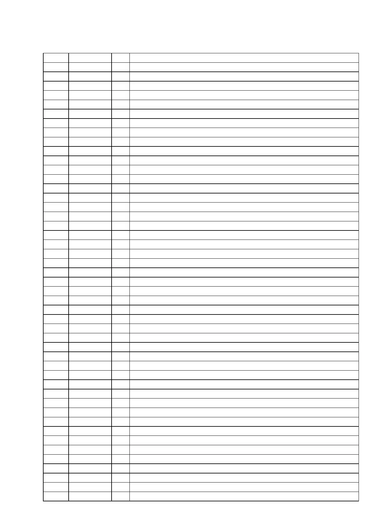
Pin No. Pin Name I/O Description
86 MDQM2 O Byte read /write mask signal 2 output
87 VDD25 — Power supply terminal (+3.3V) (SDRAM I/O signal)
88 to 95 MD20 to MD27 I/O SDRAM data
96 GND25 — Ground terminal (SDRAM I/O signal)
97 MDQM3 O Byte read /write mask signal 3 output
98 VDD25 — Power supply terminal (+3.3V) (SDRAM I/O signal)
99 to 102 MD28 to MD31 I/O SDRAM data
103 GND25 — Ground terminal (SDRAM I/O signal)
104 VDD25 — Power supply terminal (+3.3V) (SDRAM I/O signal)
105 VCLK I/O System clock (not used)
106 XCK_I/O_SEL I/O 5.1ch/downmix switch signal output
107 VS O S1 signal output
108 I/P SW O Progressive/interlace switch signal output
109 CDSEL O CD-DA selection signal output
110 MREQ O Audio muting request signal output
111 VDDP — Power supply terminal (+3.3V) (I/O signal)
112 GNDP — Ground terminal (I/O signal)
113 MDI O Serial data output to the D/A converter
114 MC O Serial data clock output to the D/A converter
115 ML O Latch enable signal output to the D/A converter
116 HIRQ2_ I Busy signal input from the EEPROM
117 VDAC_4B — Video DAC bias bit 4 (connected to the ground)
118 VDAC_VDD4 — Power supply terminal (+3.3V) (Video DAC 4)
119 VDAC_4 O VDAC output 4
120 VDAC_3B — Video DAC bias bit 3 (connected to the ground)
121 VDAC_VDD3 — Power supply terminal (+3.3V) (Video DAC 3)
122 VDAC_3 O VDAC output 3
123 VDAC_2B — Video DAC bias bit 2 (connected to the ground)
124 VDAC_VDD2 — Power supply terminal (+3.3V) (Video DAC 2)
125 VDAC_2 O VDAC output 2
126 VDAC_1B — Video DAC bias bit 1 (connected to the ground)
127 VDAC_VDD1 — Power supply terminal (+3.3V) (Video DAC 1)
128 VDAC_1 O VDAC output 1
129 VDAC_0B — Video DAC bias bit 0 (connected to the ground)
130 VDAC_VDD0 — Power supply terminal (+3.3V) (Video DAC 0)
131 VDAC_0 O VDAC output 0
132 VDAC_DVSS — Ground terminal (Video DAC digital system)
133 VDAC_DVDD — Power supply terminal (+3.3V) (Video DAC digital system)
134 VDAC_REFVDD — Power supply terminal (Video DAC reference)
135 VDAC_REF I Reference voltage input terminal(for Video DAC)
136 VDAC_REFVSS — Ground terminal (Video DAC reference)
137 XVSS — Ground terminal (crystal oscillator)
138 XOUT O Crystal oscillation signal output
139 XIN I Crystal oscillation signal input
140 XVDD — Power supply terminal (crystal oscillator)
141 AVSS2 — Ground terminal (analog PLL)
142 AVDD2 — Power supply terminal (+3.3V) (analog PLL)