– 13 – – 14 – – 15 – – 16 –
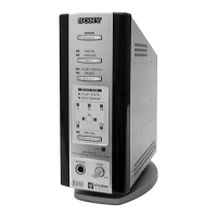
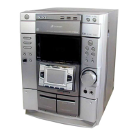
DP-IF5000
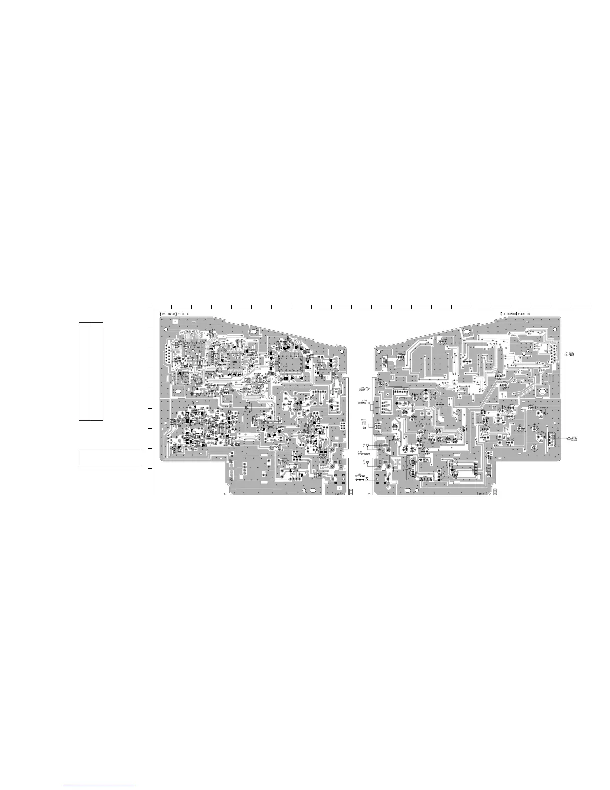
5-3. PRINTED WIRING BOARD — PROCESSOR, TRANSMITTER SECTION —
TP L
TP R
( )
( )
1
A
B
C
D
E
F
G
H
I
2345678910111213141516171819202122
Note:
• X : parts extracted from the component side.
•
®
: Through hole.
• b : Pattern from the side which enables seeing.
(The other layer’s patterns are not indicated.)
Caution:
Pattern face side: Parts on the pattern face side seen from the
(Side B) pattern face are indicated.
Parts face side: Parts on the par ts face side seen from the
(Side A) parts face are indicated.
D1 G-3
D51 F-3
D101 H-9
D102 H-9
IC1 F-4
IC101 F-9
IC102 F-6
IC103 E-8
IC105 B-3
IC201 D-2
IC202 D-3
IC204 E-4
IC301 C-7
IC302 C-5
IC303 D-6
IC304 E-6
(IC305) C-12
(IC801) H-14
(IC802) I-7
(IC803) C-12
(IC804) I-14
(IC805) H-17
Q1 G-3
Q2 H-2
Q31 F-3
Q32 G-3
Q33 F-5
Q34 F-4
Q35 G-4
Q36 G-5
Q51 F-3
Q52 F-2
Q101 F-9
Q102 G-9
Q803 H-8
• Semiconductor
Location
Ref. No. Location
( ) : SIDE B
(Page 25)
(Page 22)
(Page 22)
 Loading...