– 17 – – 18 – – 19 –
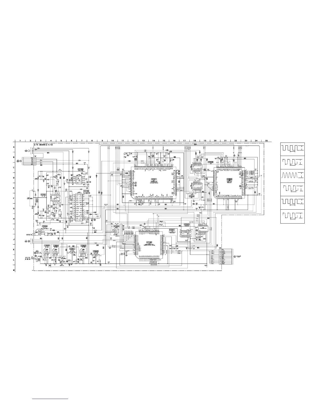
DP-IF5000
5-4. SCHEMATIC DIAGRAM — PROCESSOR SECTION — • Refer to page 27 for IC Block Diagrams.
B
Note:
• All capacitors are in µF unless otherwise noted. pF: µµF
50 WV or less are not indicated except for electrolytics
and tantalums.
• All resistors are in Ω and
1
/
4
W or less unless otherwise
specified.
• C : panel designation.
• U : B+ Line.
• Total current is measured with Power ON/OFF mode.
• Power voltage is dc 9 V and fed with regulated dc power
supply from external power voltage jack.
• Voltage and waveforms are dc with respect to ground
under no-signal conditions.
no mark : POWER ON
∗
: Impossible to measure
• Voltages are taken with a VOM (Input impedance 10 MΩ).
Voltage variations may be noted due to normal produc-
tion tolerances.
• Waveforms are taken with a oscilloscope.
Voltage variations may be noted due to normal produc-
tion tolerances.
• Circled numbers refer to waveforms.
• Signal path.
F : ANALOG
c : DIGITAL
• Waveforms
1
2
3
4
5
IC102
!§
(LRCK)
IC202
2
IC301
(¡
(SCKA)
IC301
(™
(WSA)
6
IC302
@¶
EXTAL
5Vp-p
80µsec
6.2Vp-p
IC102
!¶
(BCKIN)
4.5Vp-p
1.3µsec
12.288MHz
4Vp-p
13µsec
3.4Vp-p
80µsec
6.2Vp-p
0.7µsec
(Page 20)
(Page
26)
(Page 20)
(Page 23)
 Loading...