– 20 – – 21 – – 22 –
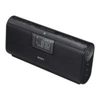
DP-IF5000
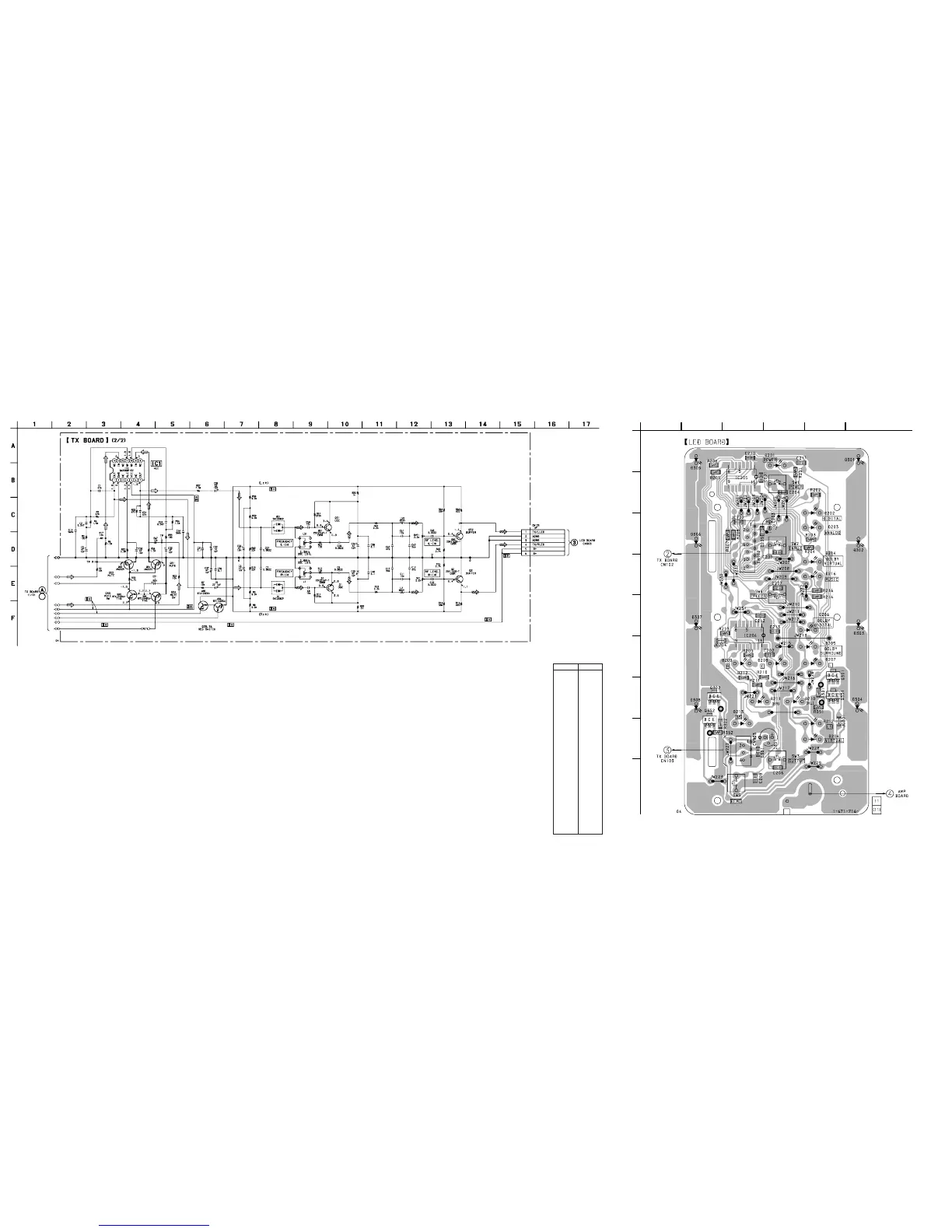
5-5. SCHEMATIC DIAGRAM — TRANSMITTER SECTION — • Refer to page 27 for IC Block Diagrams.
B
TP05
TP06
TP03
TP04
D301-304
INFRARED
EMITTER
(L-CH)
D305-308
INFRARED
EMITTER
(R-CH)
1
A
B
C
D
E
F
G
H
I
23456
5-6. PRINTED WIRING BOARD — LED SECTION —
Note:
• All capacitors are in µF unless otherwise noted. pF: µµF
50 WV or less are not indicated except for electrolytics
and tantalums.
• All resistors are in Ω and
1
/
4
W or less unless otherwise
specified.
• U : B+ Line.
• H : adjustment for repair.
• Power voltage is dc 9 V and fed with regulated dc power
supply from external power voltage jack.
• Voltage is dc with respect to ground under no-signal
condition.
no mark : POWER ON
• Voltages are taken with a VOM (Input impedance 10 MΩ).
Voltage variations may be noted due to normal produc-
tion tolerances.
• Signal path.
F : ANALOG
J : RF
Note:
• X : parts extracted from the component side.
• b : Pattern from the side which enables seeing.
D201 A-4
D202 C-5
D203 C-5
D204 H-5
D205 F-5
D206 E-5
D207 F-5
D208 F-4
D209 F-3
D210 G-4
D211 G-3
D212 H-5
D213 H-3
D214 D-5
D216 D-5
D301 A-6
D302 C-6
D303 E-6
D304 G-6
D305 A-2
D306 C-2
D307 E-2
D308 G-2
IC205 B-3
IC206 E-3
Q301 F-5
Q302 G-2
Q351 G-5
Q352 H-2
• Semiconductor
Location
Ref. No. Location
(Page
17)
(Page 23)
(Page 16)
(Page 16)
(Page 25)
 Loading...