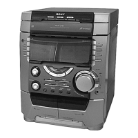
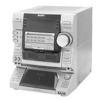
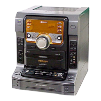
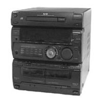
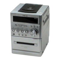
HCD-BX7/DX7/DX7J
2121
SECTION 7
DIAGRAMS
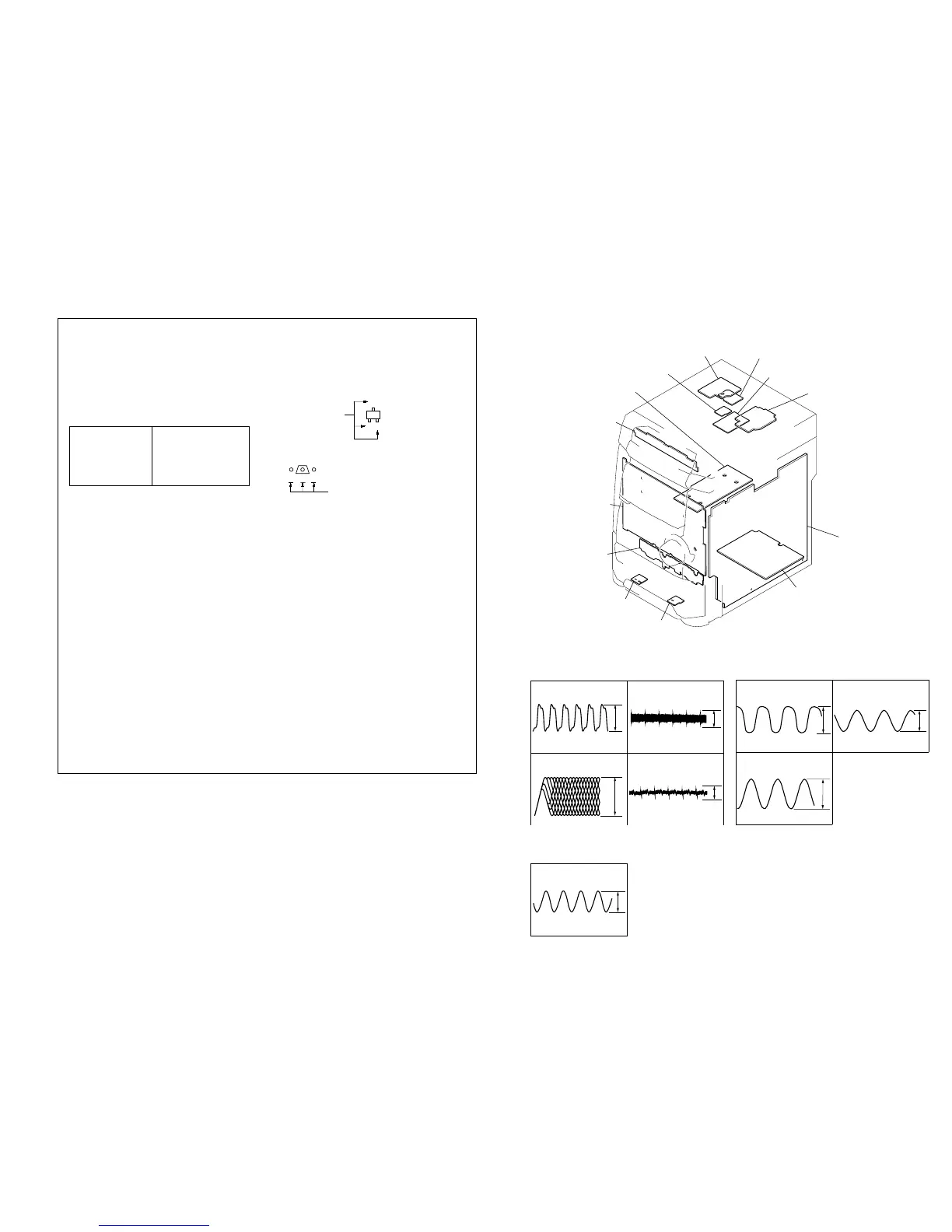
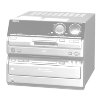
7-1. CIRCUIT BOARD LOCATION
Note on Schematic Diagram:
• All capacitors are in µF unless otherwise noted. pF: µµF
50 WV or less are not indicated except for electrolytics
and tantalums.
• All resistors are in Ω and
1
/
4
W or less unless otherwise
specified.
•
f
: internal component.
• C : panel designation.
Note on Printed Wiring Boards:
• X : parts extracted from the component side.
• b : Pattern from the side which enables seeing.
• Indication of transistor.
Note:
The components identi-
fied by mark ! or dotted
line with mark ! are criti-
cal for safety.
Replace only with part
number specified.
Note:
Les composants identifiés par
une marque ! sont critiques
pour la sécurité.
Ne les remplacer que par une
piéce portant le numéro
spécifié.
• U : B+ Line.
• V : B– Line.
• H : adjustment for repair.
• Voltages and waveforms are dc with respect to ground
under no-signal (detuned) conditions.
• Voltages are taken with a VOM (Input impedance 10 MΩ).
Voltage variations may be noted due to normal produc-
tion tolerances.
• Waveforms are taken with a oscilloscope.
Voltage variations may be noted due to normal produc-
tion tolerances.
• Circled numbers refer to waveforms.
• Signal path.
F : FM
f : AM
E : PB (DECK A)
d : PB (DECK B)
G : REC (DECK B)
J : CD
c : digital out
• Abbreviation
CND : Canadian model
AUS : Australian model
G : German model
EA : Saudi Arabia model
MY : Malaysia model
SP : Singapore model
TH : Thai model
KR : Korea model
MX : Mexican model
AR : Argentina model
E2 : Central and South AMERICA
E3 : Middle and Near East
THIS NOTE IS COMMON FOR PRINTED WIRING BOARDS AND SCHEMATIC DIAGRAMS.
(In addition to this, the necessary note is printed in each block.)
B
These are omitted.
CE
Q
PANEL Board
LEAF SW Board
HEAD (A) Board
HEAD (B) Board
TRANS Board
CD SWITCH Board
SUB-TRANS Board
BD Board
DRIVER Board
MOTOR Board
SENSOR Board
MAIN Board
POWER AMP Board
• WAVEFORMS
C
B
These are omitted.
E
Q
1 IC101 yj
CD PLAY MODE
6.4Vp-p
16.9344MHz
1.2Vp-p
2 IC101 ta
CD PLAY MODE
3 IC101 ra
CD PLAY MODE
4 IC101 el
CD PLAY MODE
400nsec/div
approx 200mVp-p
approx 170mVp-p
1 IC401 qa
STOP MODE
3.0Vp-p
32.768kHz
3.4Vp-p
2 IC401 qd
STOP MODE
3 T301 4
TAPE B REC MODE
16MHz
120Vp-p
80.7kHz
1
IC601 oa
STOP MODE
4.8Vp-p
12.5MHz
– BD BOARD –– MAIN BOARD –
– PANEL BOARD –