44
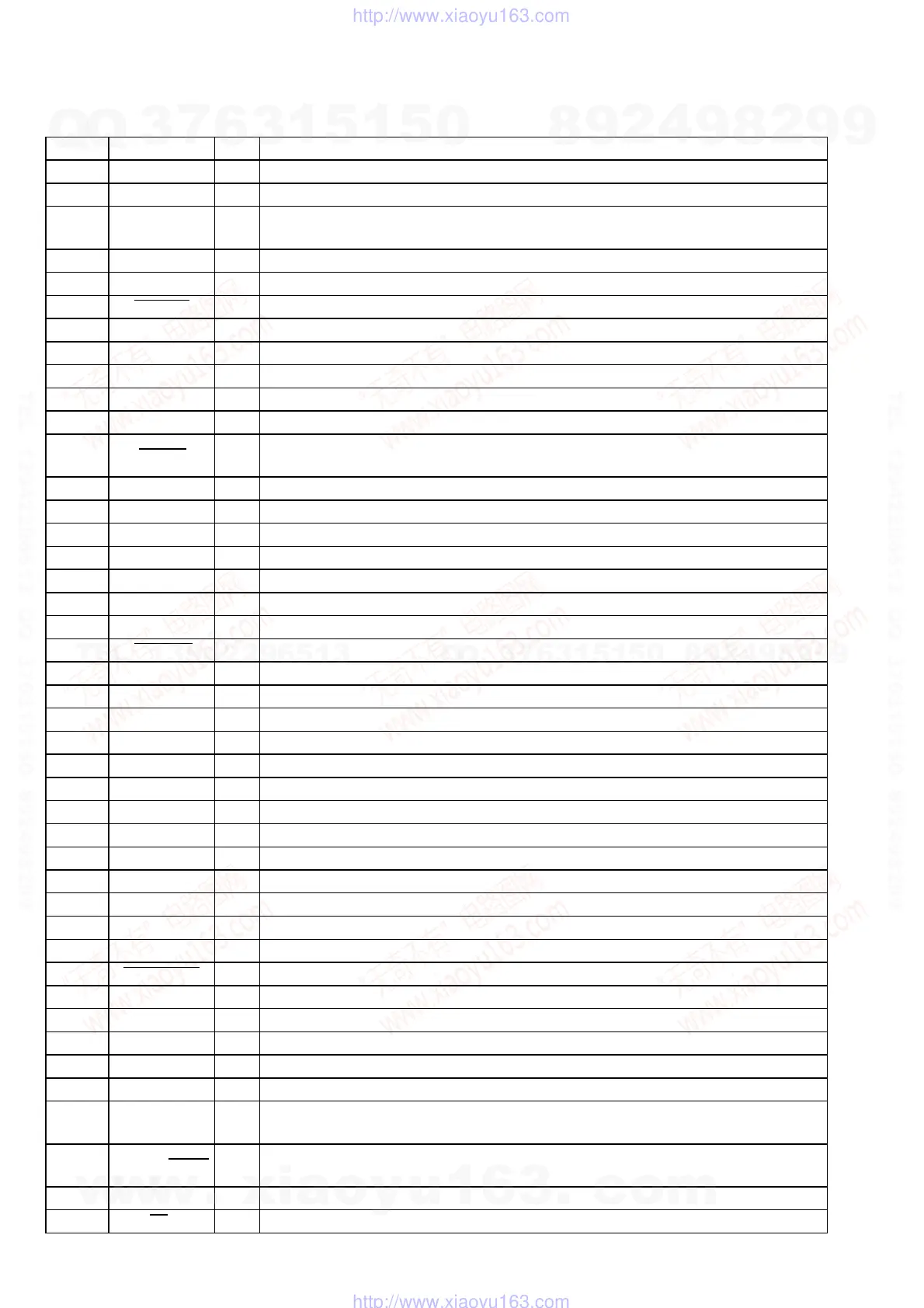
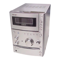
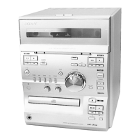
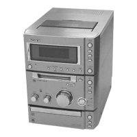
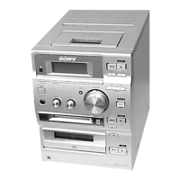
HCD-CPX1
6-19. IC PIN FUNCTION DESCRIPTION
• MAIN BOARD IC401 M30622MGN-B08FP (SYSTEM CONTROLLER (CD MECHANISM CONTROL))
Pin No. Pin Name I/O Description
1 LCD ON O
Power on/off control signal output for liquid crystal display “H”: power on
2 RDS DATA I
Serial data input from the RDS decoder Not used
3 LCD CD O
Signal output for discriminating between command and display data to the liquid crystal display
driver “L”: display data, “H”: command
4
SIRCS IN/WAKE
I
Remote control signal input terminal
5 LCD DATA O
Serial data output to the liquid crystal display driver
6 LCD CS O
Chip select signal output to the liquid crystal display driver “L” active
7 LCD CLK O
Serial data transfer clock signal output to the liquid crystal display driver
8
BYTE — Not used
9
CNVSS — Ground terminal
10 XCIN I
Sub system clock input terminal (32.768 kHz)
11 XCOUT O
Sub system clock output terminal (32.768 kHz)
12 RESET I
System reset signal input from the reset signal generator “L”: reset
For several hundreds msec. after the power supply rises, “L” is input, then it changes to “H”
13 XOUT O
Main system clock output terminal (16 MHz)
14 VSS —
Ground terminal
15 XIN I
Main system clock input terminal (16 MHz)
16 VCC —
Power supply terminal (+3.3V)
17
NMI
I
Non-maskable interrupt input terminal Not used
18 RDS CLK I
Serial data transfer clock signal input from the RDS decoder Not used
19 CD SCOR
I Subcode sync (S0+S1) detection signal input from the digital signal processor
20 AC CUT I
AC off detection signal input from the reset signal generator “L”: AC cut checked
21 ST MUTE O
Tuner muting on/off control signal output to the tuner unit “H”: muting on
22 ST CE O
PLL chip enable signal output to the tuner unit
23 ST DATA OUT O
PLL serial data output to the tuner unit
24 CD PWM3 O
RFDC PWM signal output to the RF amplifier
25 ST DATA IN I
PLL serial data input from the tuner unit
26 CD PWM2 O
PWM signal output to the RF amplifier
27 ST CLK O
PLL serial data transfer clock signal output to the tuner unit
28 CD PWM1 O
Focus servo drive PWM signal output to the RF amplifier
29 IIC CLK I/O
Communication data transfer clock signal input/output terminal Not used
30 IIC DATA I/O
Communication data bus terminal Not used
31 NO USE —
Not used
32
CD SQSO
I
Subcode Q data input from the digital signal processor
33
CD SQCLK
O
Subcode Q data reading clock signal output to the digital signal processor
34 ST STEREO I
FM stereo detection signal input from the tuner unit “L”: stereo
35
CD DATA
O
Serial data output to the digital signal processor
36 CD XLT
O Serial data latch pulse signal output to the digital signal processor
37 CD CLK O
Serial data transfer clock signal output to the digital signal processor
38 TC PLAY SW I
Head position detect switch input terminal
39 32K OUT O
Clock (32.768 kHz) signal output terminal Not used
40
TC LINE MUTE O
Line muting on/off control signal output to the recording/playback equalizer amplifier
“H”: muting on
41
TC REC/MUTE O
Recording muting on/off control signal output to the recording/playback equalizer amplifier
“L”: muting on
42 TC BIAS-ON O
Recording bias on/off control signal output terminal “H”: bias on
43 TC PB/REC O
Recording/playback selection signal output terminal “L”: playback, “H”: recording
w
w
w
.
x
i
a
o
y
u
1
6
3
.
c
o
m
Q
Q
3
7
6
3
1
5
1
5
0
9
9
2
8
9
4
2
9
8
T
E
L
1
3
9
4
2
2
9
6
5
1
3
9
9
2
8
9
4
2
9
8
0
5
1
5
1
3
6
7
3
Q
Q
TEL 13942296513 QQ 376315150 892498299
TEL 13942296513 QQ 376315150 892498299
http://www.xiaoyu163.com
http://www.xiaoyu163.com