59
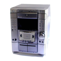
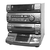
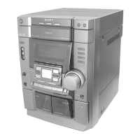
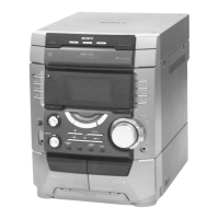
HCD-DP900D
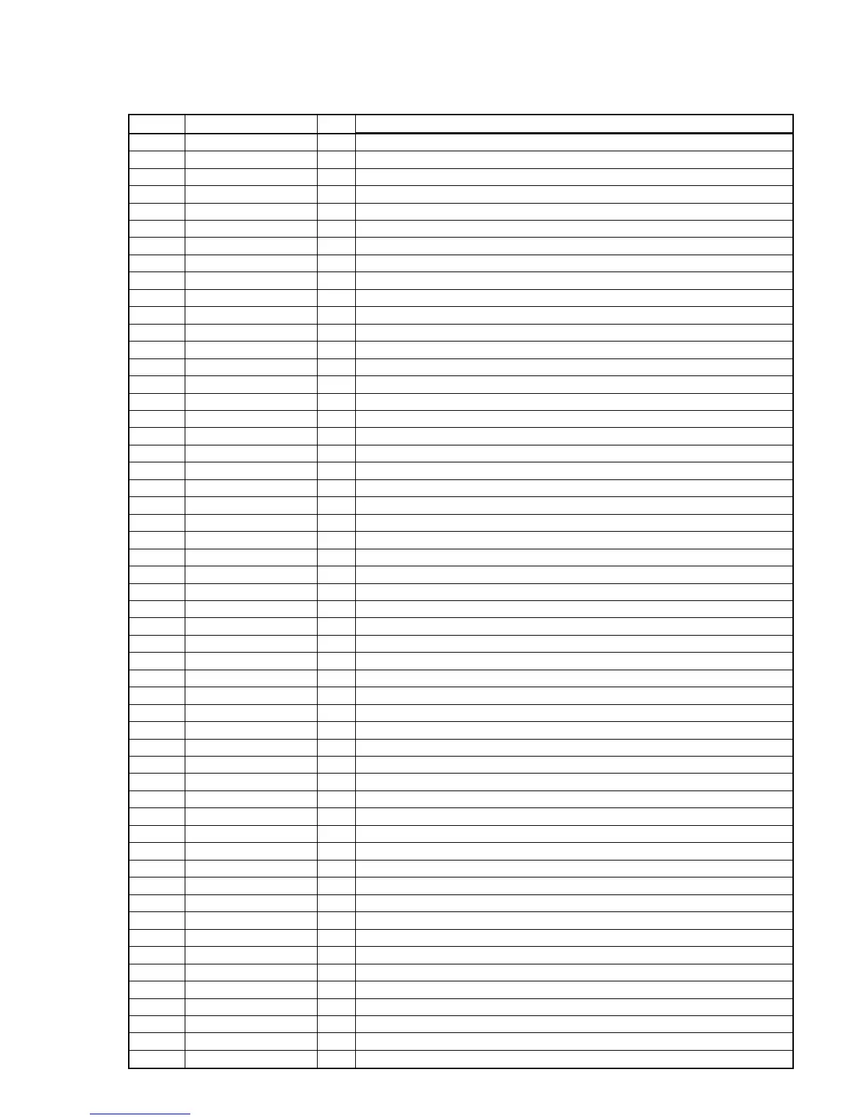
• IC601 DECODER (CXD9617R) (DSP Board (1/2))
Description
Pin NamePin No. I/O
1 VSS — Ground
2 XRST I Reset signal input
3 EXTIN — GND
4 FS2 I Sampling frequency switching signal input (Not used)
5 VDDI I Power supply
6 FS1 I Sampling frequency switching signal input (Not used)
7 PLOCK O Internal PLL lock signal output (Not used)
8 VSS — Ground
9 MCLK1 I Clock signal input (135 MHz)
10 VDDI I Power supply
11 VSS — Ground
12 MCLK2 O Clock signal output
13 M/S I Switching of master/slave operation (Not used)
14 SCKOUT O Internal system clock signal output
15 LRCKI1 I/O Sampling clock input/output for audio IF serial data (Not used)
16 VDDE — Power supply
17 BCKI1 I/O Bit clock input/output terminal for audio IF serial data (Not used)
18 SDI1 I Audio IF data input
19 LRCKO O Sampling clock output for audio IF serial data
20 BCKO O Bit clock output terminal for audio IF serial data
21 VSS — Ground
22 KFSIO I/O Audio clock signal (364fs/256fs) input/output
23 to 26 SDO1 - SDO4 O Audio IF serial data output
27 SPDIF O S/D IF output (Not used)
28 LRCKI2 I Sampling clock input for audio IF serial data
29 BCKI2 I Bit clock input terminal for audio IF serial data
30 SDI2 I Audio IF data input
31 VSS — Ground
32 HACN O Acknowledge signal output for host IF
33 HDIN I Serial data input for host IF
34 HCLK I Clock input for host IF
35 HDOUT O Serial data output for host IF
36 HCS I Chip select input for host IF
37 SDCLK O SDRAM clock output (Not used)
38 CLKEN O SDRAM clock enable signal output (Not used)
39 RAS O Raw address strobe signal output (Not used)
40 VDDI I Power supply
41 VSS — Ground
42 CAS O Column address strobe output (Not used)
43 DQM/OE0 O Data input /output mask signal output (Not used)
44 CS0 O External memory chip select (SRAM)
45 WE0 O SRAM write enable output
46 VDDE I Power supply
47 WMD1 I External memory wait mode signal input (Not used)
48 VSS — Ground
49 WMD0 I External memory wait mode signal input (Not used)
50 PAGE2 O External memory page switching signal output (Not used)
51 VSS — Ground
52 PAGE1 O External memory page switching signal output (Not used)
53 PAGE0 O External memory page switching signal output (Not used)
54 BOOT I Boot mode control signal input (Not used)
55 BTACT O Boot mode state display signal output (Not used)
56 BST I Boot stop signal input
57 MOD1 I Operation mode signal input (Not used)