58
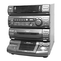
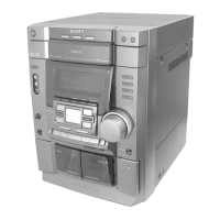
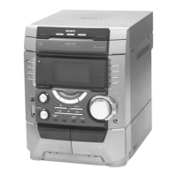
HCD-DP900D
1 FIP/LED16 O Grid drive signal output to the fluorescent indicator
2 to 5 FIP17 - 20 O Grid drive signal output to the fluorescent indicator
6 to 10 FIP21-25 O Segment drive signal output the flourescent indicator tube
11 VSS IO — Ground
12 to 22 FIP26-36 O Segment drive signal output the flourescent indicator tube
23 VDD FIP I Power supply terminal (B+ VFT)
24 to 41 FIP37-54 O Segment drive signal output the flourescent indicator tube
42 VSS IO — Ground
43 to 47 FIP35-59 O Segment drive signal output the flourescent indicator tube
48 VKK I Power supply terminal (B- for VFT)
49 MD0 I Chip Mode Select 0
50 MD1 VDD-VFT I Chip Mode Select 1
51 MD2 I Chip Mode Select 2
52 LED15 O LED switch signal output
53 LED14 O LED switch signal output
54 LED13 O LED switch signal output
55 LED12 O LED switch signal output
56 VOL A I Jog dial pulse input from the rotary encoder(A phase input)
57 VOL B I Jog dial pulse input from the rotary encoder(B phase input)
58 HEADPHONE I HEAD PHONE check (“H” head phone)
59 LED11 O LED switch signal output
60 I2C DATE O IIC data bus SDA signal
61 I2C CLA O IIC data bus reading clock signal
62 AVCC I Power supply terminal (analog)
63 AVSS — Ground (analog)
64 to 66 KEY0 - KEY2 I KEY in terminal (A/D input)
67 LED10 O LED switch signal output
68 VL I/O Touch pad control signal input/output
69 VH I/O Touch pad control signal input/output
70 HL I/O Touch pad control signal input/output
71 HH I/O Touch pad control signal input/output
72 AHH I Touch pad signal input(A/D input)
73 AHL I Touch pad signal input(A/D input)
74 AVH I Touch pad signal input(A/D input)
75 AVL I Touch pad signal input(A/D input)
76 LED9 O LED switch signal output
77 RSTX I System reset signal input
78 LED8 O LED switch signal output
79 LED7 O LED switch signal output
80 LED6 O LED switch signal output
81 VSS CPU — Ground
82 XO O Clock output (4MHz)
83 XI I Clock input (4MHz)
84 VCC - CPU I Power supply terminal
85 LED5 O LED switch signal output
86 LED4 O LED switch signal output
87 LED3 O LED switch signal output
88 LED2 O LED switch signal output
89 LED1 O LED switch signal output
90 to 100 FIP LED5 - 15 O Grid drive signal output to the fluorescent indicator
Pin Name
Pin No.
I/O
• IC1101 DISPLAY CONTROL (MB90M407APF-G-115-BND) (PANEL Board (1/2))
Discription