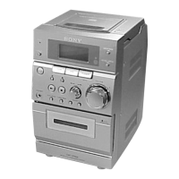
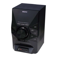
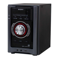
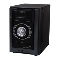
29
HCD-EP404
6-12. IC Pin Function Description
• IC301 µPD780306GC-A68-8EU System Controller, Liquid Crystal Display Driver (DISPLAY Board)
Pin No.
1
2
3
4
5
6
7
8
9
10, 11
12
13
14
15
16
17
18
19
20
21
22
23 to 26
27
28 to 30
31
32 to 59
60
61
62
63
64
65
66
67
68
69
70
71
72
73
74
75
76
77
78
79
80
81
82
I/O
I
I
I
I
I
I
I
–
–
O
–
O
I/O
O
O
O
O
O
O
O
O
O
O
I
–
O
O
O
O
O
O
–
I
–
I
I
I
I
I
O
O
I/O
I
O
–
I
O
–
I
Pin Name
KEY2
KEY3
KEY4
KEY5
ANALYSER
STATION
RDSDATA
AVDD
AVREF
CDOUT1, CDOUT2
VSS
TIME
CDDATA
CDRESET
REC-EN
INPINENA
REC-LED
SOUNDENA
PLLENA
MUTE
POWER
COM0 to COM3
BIAS
VLC0 to VLC2
VSS
LCD4 to LCD31
LCD32
LCD33
LCD34
LCD35
LCD36
NC
24/12
NC
AMS
RDS
BLINK
REC_RVS
DATAIN
DATAOUT
CLK
EEPROMDATA
STEREO
EEPROMCLK
VSS
X1
X2
VDD
XT1
Description
Key input terminal (A/D input) SW306 to SW309 (x , X , N , TUNER MEM/ENTER)keys input
Key input terminal (A/D input) SW310 to SW312 (PRESET +/–, DISPLAY)keys input
Key input terminal (A/D input)
SW313 to SW315 (TUNING – . m , TUNING + M >, MUSIC MENU)keys input
Key input terminal (A/D input) SW316, SW317 (MEGA BASS, z )keys input
Analyzer level detection signal input terminal (A/D input) Not used (open)
Tuning detection signal input from the LA1823 (IC101)(A/D input)
Selection data input from the Q301
Power supply terminal
Reference voltage input terminal for A/D converter
Not used (open)
Ground terminal
LED control signal output
Two-way data bus with the CD block
Reset signal output to the CD block “L ”:reset
Recording bias switch control signal output
Mega bass on/off selection signal output “H ”:mega bass on
LED control signal output
Function switch and electronic volume LC75392 (IC401) chip enable signal output
PLL chip enable signal output to the FM/AM PLL (IC102) “H ” active
Audio line muting on/off control signal output “H ”:muting on
System power on/off control signal output “H ”:power on
Common drive signal output to the liquid crystal display
Bias output for the liquid crystal display drive
Input terminal for liquid crystal display drive voltage
Ground terminal
Segment drive signal output to the liquid crystal display
Segment drive signal output to the liquid crystal display Mode selection signal output
Segment drive signal output to the liquid crystal display Mode selection signal output
Segment drive signal output to the liquid crystal display Mode selection signal output
Segment drive signal output to the liquid crystal display Mode selection signal output
Segment drive signal output to the liquid crystal display
Not used (open)
Mode switch detection signal input
Not used (open)
Half switch detection signal input
Not used (open)
Rec-proof switch detection signal input
Not used
Serial data input from the FM/AM PLL (IC102)
Serial data output to the FM/AM PLL (IC102) and LC75392 (IC401)
Serial data transfer clock signal output to the FM/AM PLL (IC102) and LC75392 (IC401)
Two-way data bus with the EEPROM (IC302)
FM stereo detection signal input from the LA1823 (IC101) “L ”:stereo
Clock signal output to the EEPROM (IC302)
Internal connection terminal (connected to ground)
Main system clock output terminal (4.194304 MHz)
Main system clock input terminal (4.194304 MHz)
Power supply terminal
Sub system clock input terminal (32.768 kHz) Not used (open)