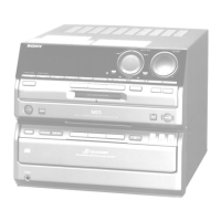
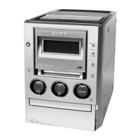
– 111 –
41 WFCK O
WFCK clock (7.35 kHz) signal output (Playback: EFM decoder PLL, Recording: EFM encoder PLL)
(Open)
42 GTOP O “H”: Playback EFM frame sync protect window opens. Not used (Open).
43 GFS O “H”: Playback EFM frame sync is synchronized with interpolation protect timing. Not used (Open).
44 XPLCK O
EFM decoder PLL clock output (98Fs=4.3218 MHz)
Falling edge are synchronized with EFM signal edge (Open)
45 EFMO O EFM signal output (Recording)
46 RAOF O
Overflow detection signal output of the internal RAM (Decoder monitor output).
“H” is output when the disc rotation exceeds ± 4F jitter margin during playback. Not used (Open).
47 MVCI I Digital In PLL oscillation input. Not used (Connected to GND).
48 TEST2 I Test pin (Connected to GND).
49 DIPD O (3)
Digital In PLL phase comparison output. When internal VCO: (frequency: Low→ “H”), external
VCO: (frequency: Low→ “L”).
50 DVSS — GND (Digital system)
51 DICV I (A) Internal VCO control voltage input for the digital In PLL.
52 DIFI I (A) Filter input when the internal VCO for the digital In PLL is used.
53 DIFO O (A) Filter output when the internal VCO for the digital In PLL is used.
54 AVDD — Power supply (+5V) (Analog)
55 ASYO O Playback EFM full swing output (L=VSS, H=VDD)
56 ASYI I (A) Playback EFM asymmetry comparator voltage input
57 BIAS I (A) Playback EFM asymmetry circuit constant-current input
58 RFI I (A) Playback EFM RF signal input from the CXA1981AR (IC101).
59 AVSS — GND (Analog)
60 CLTV I (A) VCO control voltage input for the decoder PLL master clock PLL.
61 PCO O (3) Phase comparison output for the decoder PLL master clock PLL.
62 FILI I (A) Filter input for the decoder PLL master clock PLL.
63 FILO O (3) Filter output for the decoder PLL master clock PLL.
64 PEAK I (A) Peak hold signal of light amount signal input from the CXA1981AR (IC101).
65 BOTM I (A) Bottom hold signal of light amount signal input from the CXA1981AR (IC101).
66 ABCD I (A) Light amount signal input from the CXA1981AR (IC101).
67 FE I (A) Focus error signal input from the CXA1981AR (IC101).
68 AUXI I (A) Auxiliary signal input from the CXA1981AR (IC101).
69 VC I (A) Middle point voltage (+2.5V) input from the CXA1981AR (IC101).
70 ADIO O (A) Monitor output of A/D converter input signal. Not used (Open).
71 TEST3 I (A) Test pin (Connected to ground.)
72 AVDD — Power supply pin (+5V) (Analog)
73 ADRT I (A) A/D converter operational range upper limit voltage input (Connected to AVDD.)
74 ADRB I (A) A/D converter operational range lower limit voltage input (Connected to ground.)
75 AVSS — GND (Analog)
76 SE I (A) Sled error signal input from the CXA1981AR (IC101).
77 TE I (A) Tracking error signal input from the CXA1981AR (IC101).
78 AUX2 I (A) Auxiliary input pin 2. Not used (Connected to ground).
79 DCHG I (A) Connected to GND.
80 APC I (A) Laser APC input . Not used (Connected to ground).
81 TEST1 I Test pin (Fixed at “L” in this unit.)
82 ADFG I
ADIP duplex FM signal input from the CXA1981AR (IC101). (22.05 kHz ±1 kHz) (TTL Schmidt
input)
Pin No. Pin Name I/O Function