– 116 –
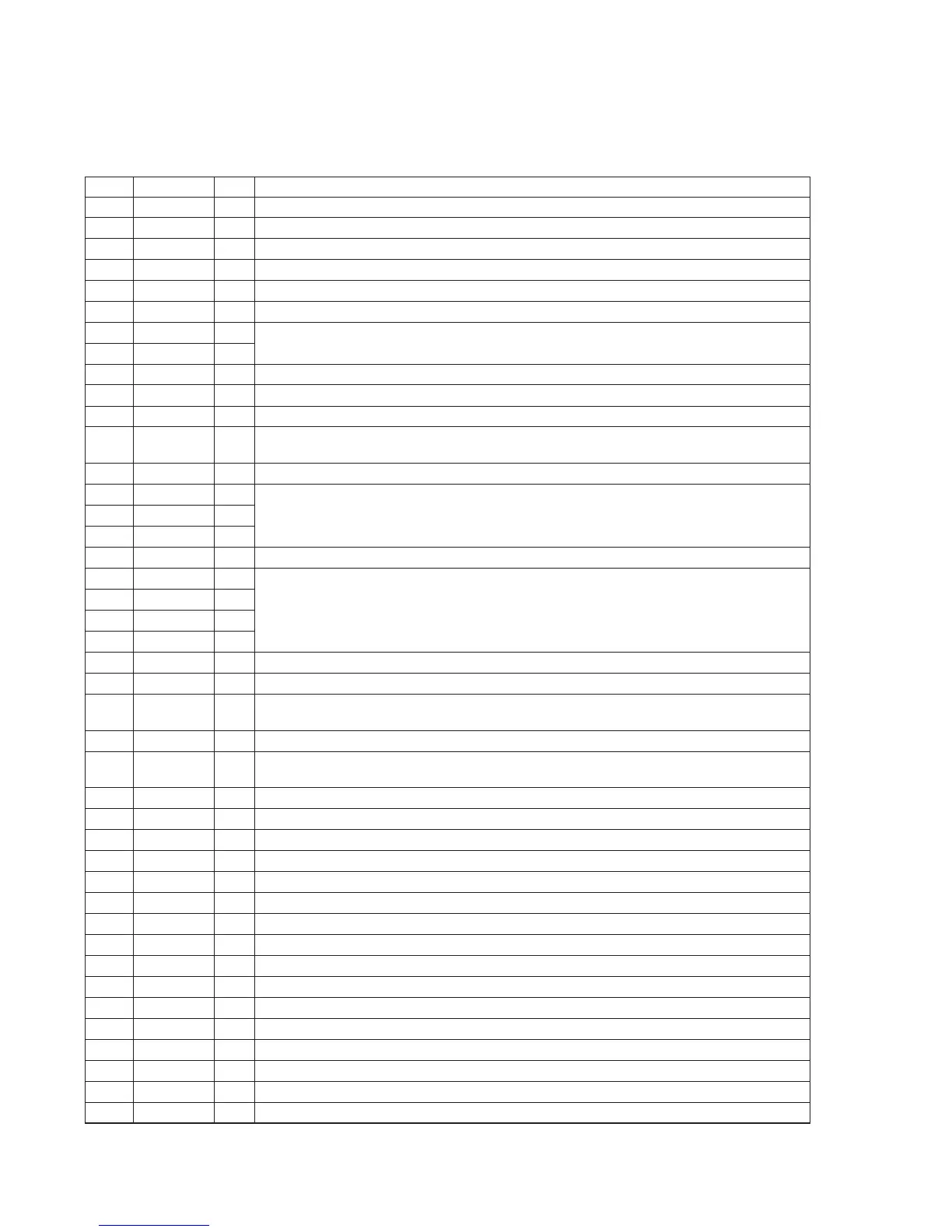
1 VDD — Power supply (+5V)
2 SWDT I Writing data signal input from the MD system control (IC201).
3 SCK I Serial clock signal input from the MD system control (IC201).
4 XLAT I Serial latch signal input from the MD system control (IC201).
5 SRDT O/Z Reading data signal output to the MD system control (IC201).
6 SENSE O/Z Internal status (SENSE) output to the MD system control (IC201).
7 SCMD0 I
8 SCMD1 I
Serial command control mode input from the MD system control (IC201).
9 XINT O Interrupt status output to the MD system control (IC201).
10 RCPB I Recording/Playback select input. Not used (Fixed at “L”).
11 WRMN I Write/Monitor mode select signal input from the MD system control (IC201).
12 TX I
Writing data transmission timing input from the MD system control (IC201).
Also serves as the magnetic head ON/OFF.
13 VSS — Ground
14 SICK I
15 IDSL I Chip reservation. Not used (Connected to ground).
16 XILT I
17 XRST I Reset signal input from the MD system control (IC201). Reset: “L”.
18 TS0 I
19 TS1 I
20 TS2 I
Test pin (Connected to GND)
21 TS3 I
22 EXIR I Chip reservation. Not used (Connected to GND).
23 SASL I Block selection when single use. “L”: ATRAC, “H”: RAM controller (Fixed at “L”.)
24 SNGLE I
Normally fixed at “L” and used for ATRAC or RAM controller. Fixed at “H” when single use.
(Fixed at “L”.)
25 VSS — Ground
26 AIRCPB O
Recording/Playback mode signal output for the ATRAC or external audio block.
Not used (Open).
27 XRQ I/O XRQ signal input/output of ATRAC I/F. Not used (Open).
28 ADTO I/O Decode data signal input/output of ATRAC. Not used (Open).
29 ADTI I/O Encode data signal input/output of ATRAC. Not used (Open).
30 XALT I/O XALT signal input/output of ATRAC I/F. Not used (Open).
31 ACK I/O ACK signal input/output of ATRAC I/F. Not used (Open).
32 AC2 I/O Error data signal input/output of ATRAC I/F. Not used (Open).
33 LCHST I/O Lch Start data signal input/output of ATRAC I/F. Not used (Open).
34 EXE I/O EXE signal input/output of ATRAC I/F. Not used (Open).
35 MUTE I/O MUTE signal input/output of ATRAC I/F. Not used (Open).
36 OSCO O Clock output (45 MHz)
37 OSCI I Clock input (45 MHz)
38 VSS — Ground
39 ATT I/O ATT signal input/output of ATRAC I/F.
40 F86 O 11.6 msec. timing signal output of ATRAC block.
41 DOUT O Monitor/Decode audio data signal output to the A/D, D/A converter (IC303).
42 ADIN I Recording signal input from the A/D, D/A converter (IC303).
Digital Board IC271 CXA2536CR (Shock Proof Memory Controller, ATRAC Encoder/Decoder)
Pin No. Pin Name I/O Function


 To Next Page