— 64 —
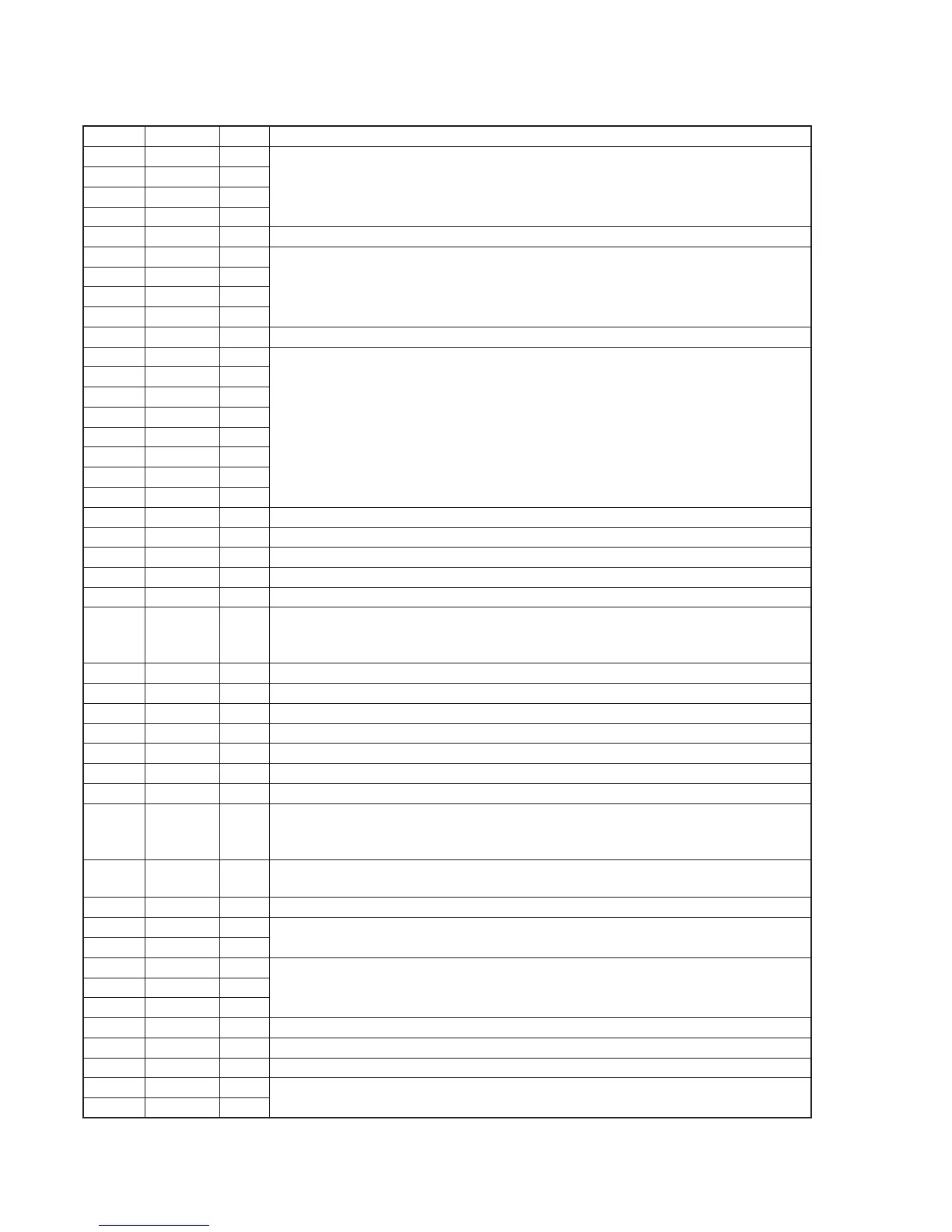
Pin No.
1
2
3
4
5
6
7
8
9
10
11
12
13
14
15
16
17
18
19
20
21
22
23
24
25
26
27
28
29
30
31
32
33
34
35
36
37
38
39
40
41
42
43
44
I/O
I
I
I
I
—
I
I
I
I
—
I
I
I
I
I
I
I
I
—
O
I
—
—
O
I
I
—
—
O
—
—
O
O
—
O
O
I
I
I
—
I
—
I
I
Description
8-bit pixel data input pins (PD0 to 7).
When control register bit “PIF MODE”=“0”, serve as input pins for multiplexed Y, Cb, Cr signals.
When control register bit “PIF MODE”=“1”, serve as input pins for Y signal.
Digital ground
8-bit pixel data input pins (PD0 to 7).
When control register bit “PIF MODE”=“0”, serve as input pins for multiplexed Y, Cb, Cr signals.
When control register bit “PIF MODE”=“1”, serve as input pins for Y signal.
Digital power supply
8-bit pixel data input pins/test data bus.
When control register bit “PIF MODE”=“0”, these input pins cannot be used.
When control register bit “PIF MODE”=“1”, serve as input pins for multiplexed Cb, Cr signals.
In the test mode, used for internal circuit test data bus.
The test mode is allowed to use only for device vendors.
Digital ground
Reference current output pin. Connect a resistor ×16 times (“16R”) of the output resistance value “R”
Voltage reference input pin. Sets the output full-scale value
Analog power supply
Analog ground
10-bit D/A converter output.
When control register bit “YC/YUV”=“1”, outputs the composite signal.
When control register bit “YC/YUV”=“0”, outputs the color difference (V) signal.
Connect to Vss with an approx. 0.1 µF capacitor
Connect to AVDD with an approx. 0.1 µF capacitor
Analog power supply
Analog ground
10 bit D/A converter output. (Luminance (Y) signal output.)
Analog power supply
Analog ground
10-bit D/A converter output.
When control register bit “YC/YUV”=“1”, outputs the chroma (C) signal.
When control register bit “YC/YUV”=“0”, outputs the color difference (U) signal.
Test data bus. In the test mode, used for internal circuit test data bus.
The test mode is allowed to use only for device vendors (Not used).
Digital power supply
Test data bus. In the test mode, used for internal circuit test data bus.
The test mode is allowed to use only for device vendors (Not used)
Test mode control input pin. Pulled-up.
When these pins are “H”, CXD1913Q is not in the test mode.
The test mode is allowed to use only for device vendors
Digital ground
Test mode reset input pin. During power on/reset, set to “L” for more than 40 clocks (SYSCLK) (Not used)
Digital power supply
Test mode control input pin. (Not used)
Pin Name
Y7
Y6
Y5
Y4
VSS
Y3
Y2
Y1
Y0
VDD
C7
C6
C5
C4
C3
C2
C1
C0
VSS
IREF
VREF
AV D D 1
AVSS1
COMPO
VB
VG
AV D D 2
AVSS2
YOUT
AV D D 3
AVSS3
COUT
TD10
VDD
TD9
TD8
XTEST1
XTEST2
XTEST3
VSS
TRST
VDD
TDI
TMS
• IC401 10 BIT VIDEO D/A CONVERTER (CXD1913Q)/VIDEO board



 To Next Page