1919
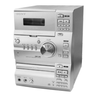
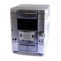
HCD-VP1
5-5. NOTE FOR PRINTED WIRING BOARDS AND SCHEMATIC DIAGRAMS
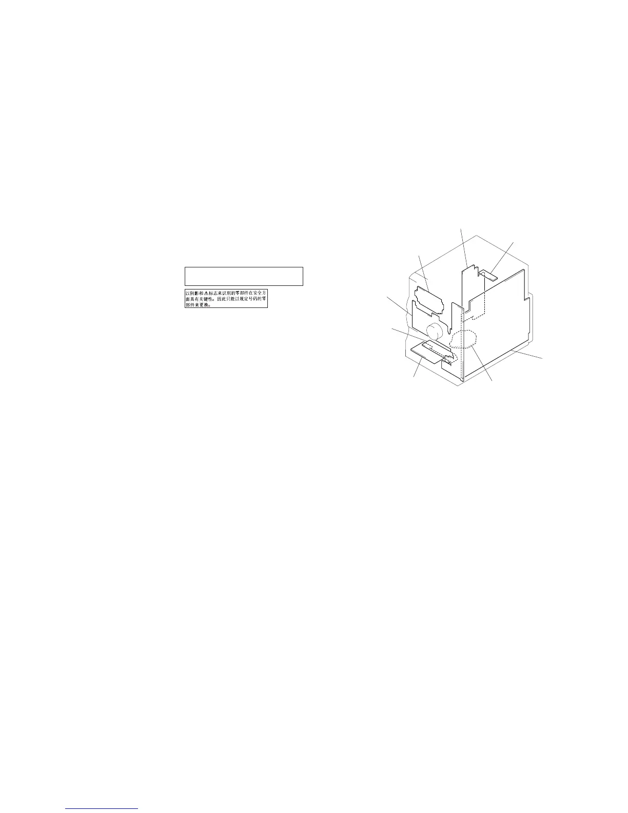
• Circuit Boards Location
Note on Printed Wiring Boards:
• X : parts extracted from the component side.
• Y : parts extracted from the conductor side.
• b : Pattern from the side which enables seeing.
Note on Schematic Diagram:
• All capacitors are in µF unless otherwise noted. pF: µµF
50 WV or less are not indicated except for electrolytics
and tantalums.
• All resistors are in Ω and
1
/
4
W or less unless otherwise
specified.
• 2 : nonflammable resistor.
• C : panel designation.
Note: The components identified by mark ! or dotted line
with mark ! are critical for safety.
Replace only with part number specified.
• U : B+ Line.
• V : B– Line.
• H : adjustment for repair.
• Voltages are taken with a VOM (Input impedance 10 MΩ).
Voltage variations may be noted due to normal produc-
tion tolerances.
• Waveforms are taken with a oscilloscope.
Voltage variations may be noted due to normal produc-
tion tolerances.
• Circled numbers refer to waveforms.
• Signal path.
F : TUNER
E : TAPE (PLAY)
a : TAPE (REC)
J : CD (AUDIO)
L : CD (VIDEO)
c : DIGITAL OUT
N : MIC IN
LCD board
POWER board
VIDEO SW board
MAIN board
HP/MIC board
LOADING board
CD board
CONTROL board
 Loading...