23
23
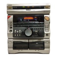
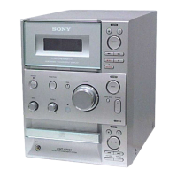
HCD-VP1
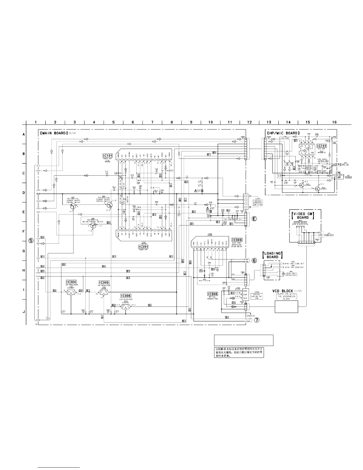
5-9. SCHEMATIC DIAGRAM – MAIN Board (2/4), HP/MIC Board, VIDEO SW Board, LOADING Board – • See page 34 for IC Block Diagrams.
The components identified by mark ! or dotted
line with mark ! are critical for safety.
Replace only with part number specified.
• Voltages and waveforms are dc with respect to ground
under no-signal (detuned) conditions.
no mark : FM
( ) : CD PLAY
[ ] : TAPE PLAY
〈〈 〉〉 : MD/VIDEO
(Page
22)
(Page 25)
(Page 30)
(Page 25)
 Loading...