Do you have a question about the Sony HCD-VX555 and is the answer not in the manual?
Details amplifier input/output specs and power ratings.
Specifications for the CD player, including laser type and frequency response.
Procedure for removing the top case of the unit during disassembly.
Instructions for disassembling the front panel section of the unit.
Detailed procedure for disassembling the base unit.
Procedure for cold reset to restore factory default settings.
Test mode for checking software version, FL tube, LED, keyboard, and VACS.
Test mode for checking Amplifier, Tuner, and Tape operations.
Mode to output color-bars and 1 kHz sine wave for video CD signal check.
Table detailing torque measurements for various modes and components.
Adjustments for tape deck sections, including azimuth and speed.
Procedure for adjusting playback level for both decks.
Diagram showing the physical location of all circuit boards within the unit.
System block diagrams illustrating the interconnections between different sections.
Printed wiring board layout for the main section of the unit.
Schematic diagram for the main section (part 1 of 4).
Detailed pin functions for integrated circuits used in the unit.
Block diagrams for key integrated circuits.
Exploded view of the cabinet section, showing assembly of outer parts.
Exploded view of the front panel section and its components.
Exploded view of the main board and its associated components.
Exploded view of the tape mechanism deck section (TCM-230MWR41C).
Exploded view of the CD mechanism deck section (CDM58E-30BD61A).
Exploded view of the base unit section (BU-30BD61A).
Notes regarding parts list, standardization, and abbreviations.
| Power Output | 100 W |
|---|---|
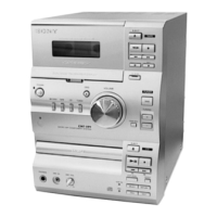
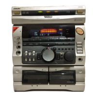
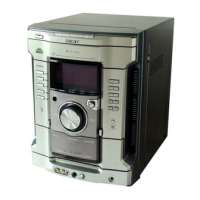
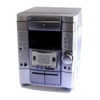
| CD Player | Yes |
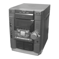
| Cassette Deck | Yes |
| Tuner | Yes |
| Tuner Bands | AM/FM |
| Speakers | 2 Speakers |
| Bluetooth | No |
| Remote Control | Yes |
| Weight | 8.5 kg |
| Type | Mini Hi-Fi System |
| Speaker Configuration | 2.0 |
| Functions | CD, Cassette, Tuner |
| Cassette Deck Type | Double Cassette Deck |