3
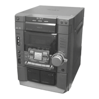
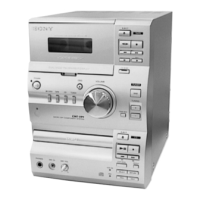
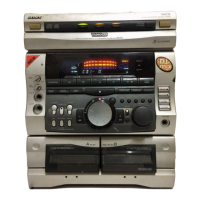
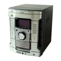
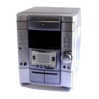
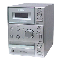
HCD-VX555/VX555J
TABLE OF CONTENTS
1. GENERAL ·········································································· 4
2. DISASSEMBLY ································································ 6
3. TEST MODE ···································································· 12
4. MECHANICAL ADJUSTMENTS ····························· 15
5. ELECTRICAL ADJUSTMENTS ······························· 15
6. DIAGRAMS ·······························································21
6-1. Circuit Board Location ················································· 22
6-2. Block Diagrams ···························································· 24
6-3. Printed Wiring Board Main Section ·························· 27
6-4. Schematic Diagram Main Section (1/4) ···················· 28
6-5. Schematic Diagram Main Section (2/4) ···················· 29
6-6. Schematic Diagram Main Section (3/4) ···················· 30
6-7. Schematic Diagram Main Section (4/4) ···················· 31
6-8. Printed Wiring Board BD Section ····························· 32
6-9. Schematic Diagram BD Section ································ 33
6-10. Printed Wiring Board AMP Section························· 34
6-11. Schematic Diagram AMP Section ··························· 35
6-12. Printed Wiring Board Panel Section ························ 36
6-13. Schematic Diagram Panel Section ··························· 37
6-14. Printed Wiring Board Panel SW Section ················· 38
6-15. Schematic Diagram Panel SW Section ···················· 39
6-16. Printed Wiring Board Leaf SW Section··················· 40
6-17. Schematic Diagram Leaf SW Section ····················· 41
6-18. Printed Wiring Board Driver Section ······················· 42
6-19. Schematic Diagram Driver Section ························· 43
6-20. Printed Wiring Board Video Section ························ 44
6-21. Schematic Diagram Video Section (1/3)·················· 45
6-22. Schematic Diagram Video Section (2/3)·················· 46
6-23. Schematic Diagram Video Section (3/3)·················· 47
6-24. Printed Wiring Board Trans Section ························ 48
6-25. Schematic Diagram Trans Section ··························· 49
6-26. Printed Wiring Board Switch Section ······················ 50
6-27. Schematic Diagram Switch Section························· 50
6-28. IC Pin Function Description ······································· 51
6-29. IC Block Diagrams ····················································· 58
7. EXPLODED VIEWS
7-1. Cabinet Section ····························································· 60
7-2. Front Panel Section······················································· 61
7-3. MAIN Board Section ···················································· 62
7-4. Tape Mechanism Section-1(TCM-230MWR41C) ······· 63
7-5. Tape Mechanism Section-2(TCM-230AWR41C) ········ 64
7-6. Tape Mechanism Section-3
(TCM-230PWR41C)(1/2) ············································ 65
7-7. Tape Mechanism Section-4
(TCM-230PWR41C)(2/2) ············································ 66
7-8. CD Mechanism Deck Section (CDM58E-30BD61A)·· 67
7-9. Base Unit Section (BU-30BD61A) ······························ 68
8. ELECTRICAL PARTS LIST ······································· 69