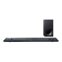
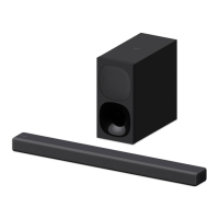
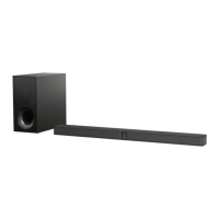
HT-NT3
65
Pin No. Pin Name I/O Description
AD27 REXT - External reference resistor connection terminal
AD28 HTPLG I Hot plug detection signal input from the HDMI ARC OUT connector
AE3 NC - Not used
AE5 DDRVCCIO1 - Power supply terminal (+1.5V)
AE6 to AE8
RDQ29, RDQ31,
RDQ30
I/O Two-way data bus with the SD-RAM
AE9 RWE_ O Write enable signal output to the SD-RAM
AE10 RODT O On die termination enable signal output to the SD-RAM
AE11 RRAS_ O Row address signal output to the SD-RAM
AE12 RA3 O Address signal output to the SD-RAM
AE13 RCSX_ - Not used
AE14 RA4 O Address signal output to the SD-RAM
AE16 RDQ11 I/O Two-way data bus with the SD-RAM
AE17 RDQM1 O Data mask signal output to the SD-RAM
AE18 RDQ13 I/O Two-way data bus with the SD-RAM
AE19,
AE20
DVCC33_IO_STB - Power supply terminal (+3.3V)
AE21 NFREN O Read enable signal output to the NAND fl ash
AE22 NFCEN2 - Not used
AE23 NFD0 I/O Two-way data bus with the NAND fl ash
AE24 NFWEN O Write enable signal output to the NAND fl ash
AE25 HTPLG_RX O Hot plug detection signal output to the HDMI IN 1 connector
AE26 PWR5V_RX2 I Power supply voltage (+5V) input from the HDMI IN 2 connector
AF1, AF2
TP_MEMPLL,
TN_MEMPLL
- Not used
AF3 NC - Not used
AF4 RDQ25 I/O Two-way data bus with the SD-RAM
AF5 DGND12_K - Ground terminal
AF6 RDQ28 I/O Two-way data bus with the SD-RAM
AF7 DDRVCCIO1 - Power supply terminal (+1.5V)
AF8, AF9 RDQ20, RDQ22 I/O Two-way data bus with the SD-RAM
AF10 DDRVCCIO1 - Power supply terminal (+1.5V)
AF11, AF12 RA9, RA5 O Address signal output to the SD-RAM
AF13 RCS_ O Chip select signal output to the SD-RAM
AF14 to
AF16
RDQ3, RDQ1, RDQ9 I/O Two-way data bus with the SD-RAM
AF17, AF18 DDRVCCIO1 - Power supply terminal (+1.5V)
AF20 RDQ5 I/O Two-way data bus with the SD-RAM
AF21 NFD6 I/O Two-way data bus with the NAND fl ash
AF22 NFCEN O Chip enable signal output to the NAND fl ash
AF23 NFD1 I/O Two-way data bus with the NAND fl ash
AF24 NFALE O Address latch enable signal output to the NAND fl ash
AF25 UARXD - Not used
AF26 RESET_ I Reset signal input from the system controller "L": reset
AF27 DDC_SDA_RX I/O Two-way I2C data bus with the HDMI IN 1 connector
AF28 DDC_SCL_RX O I2C clock signal output to the HDMI IN 1 connector
AG1 to AG4
RDQ17, RDQ16,
RDQ26, RDQ27
I/O Two-way data bus with the SD-RAM
AG5 RDQS2 O Data strobe signal (positive) output to the SD-RAM
AG6 RCLK1 O Clock signal (positive) output to the SD-RAM
AG7 RDQS3_ O Data strobe signal (negative) output to the SD-RAM
AG8 RDQ21 I/O Two-way data bus with the SD-RAM
AG10 RBA2 O Bank address signal output to the SD-RAM
AG11,
AG13
RA2, RA11 O Address signal output to the SD-RAM
 Loading...