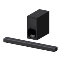
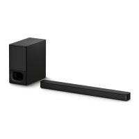
HT-NT3
70
Pin No. Pin Name I/O Description
P5 NO_USE - Not used
P6 NO_USE - Not used
P7 A1 I
Address inputs: Provided the row address for active commands and the column address for
Read/Write commands to select one location out of the memory array in the respective bank.
The address inputs also provide the op-code during Mode Register Set commands.
P8 A4 I
Address inputs: Provided the row address for active commands and the column address for
Read/Write commands to select one location out of the memory array in the respective bank.
The address inputs also provide the op-code during Mode Register Set commands.
P9 VSS - Ground
R1 VDD - Power Supply: 1.5V +/-0.075
R2 A7 I
Address inputs: Provided the row address for active commands and the column address for
Read/Write commands to select one location out of the memory array in the respective bank.
The address inputs also provide the op-code during Mode Register Set commands.
R3 A9 I
Address inputs: Provided the row address for active commands and the column address for
Read/Write commands to select one location out of the memory array in the respective bank.
The address inputs also provide the op-code during Mode Register Set commands.
R4 NO_USE - Not used
R5 NO_USE - Not used
R6 NO_USE - Not used
R7 A11 I
Address inputs: Provided the row address for active commands and the column address for
Read/Write commands to select one location out of the memory array in the respective bank.
The address inputs also provide the op-code during Mode Register Set commands.
R8 A6 I
Address inputs: Provided the row address for active commands and the column address for
Read/Write commands to select one location out of the memory array in the respective bank.
The address inputs also provide the op-code during Mode Register Set commands.
R9 VDD - Power Supply: 1.5V +/-0.075
T1 VSS - Ground
T2
RESET I
Active Low Asynchronous Reset: Reset is active when RESET is LOW, and inactive when
RESET is HIGH. RESET must be HIGH during normal operation. RESET is CMOS rail to rail
signal with DC high and low at 80% and 20% of VDD, example, 1.20V for DC high and 0.30V
for DC low.
T3 A13 I
Address inputs: Provided the row address for active commands and the column address for
Read/Write commands to select one location out of the memory array in the respective bank.
The address inputs also provide the op-code during Mode Register Set commands.
T4 NO_USE - Not used
T5 NO_USE - Not used
T6 NO_USE - Not used
T7 NC - No Connect: No internal electrical connection is present.
T8 A8 I
Address inputs: Provided the row address for active commands and the column address for
Read/Write commands to select one location out of the memory array in the respective bank.
The address inputs also provide the op-code during Mode Register Set commands.
T9 VSS - Ground
 Loading...