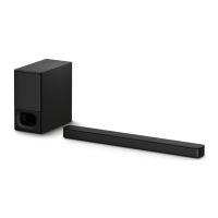
HT-NT3
69
Pin No. Pin Name I/O Description
K9 CKE I
Clock Enable: CKE HIGH activates, and CKE LOW deactivates, internal clock signal and de-
vice input buffers and output drivers. Talking CKE LOW provides Precharge Power-Down and
Self Refresh operation (all banks idle), or Active Power-Down (Row Active in any bank). CKE
is asynchronous for self refresh exit. After V
REFCA has become stable during the power on and
initialization sequence, it must be maintained during all operations (including Self-Refresh).
CKE must be maintained high throughout read and write accesses. Input buffers, excluding
CK, CK, ODT and CKE are disabled during power-down. Input buffers, excluding CKE, are
disabled during Self-Refresh.
L1 NC - No Connect: No internal electrical connection is present.
L2
CS I
Chip Select: All commands are masked when CS is registered HIGH. CS provides for external
Rank selection on system with multiple Ranks. CS is considered part of the command code.
L3
WE I Command Input: WE (along with CS) defi ne the command being entered.
L4 NO_USE - Not used
L5 NO_USE - Not used
L6 NO_USE - Not used
L7 A10 I
Address inputs: Provided the row address for active commands and the column address for
Read/Write commands to select one location out of the memory array in the respective bank.
The address inputs also provide the op-code during Mode Register Set commands.
Autoprecharge: A10 is sampled during Read/Write commands to determine whether Auto-
precharge should be performed to the accessed bank after the Read/Write operation. (HIGH:
Autoprecharge; LOW: No Autoprecharge)
A10 is sampled during a Precharge command to determine the Percharge applies to one bank
(A10 LOW) or all banks (A10 HIGH). If only one bank is to be precharged, the bank is selected
by bank adresses.
L8 ZQ - Reference Pin for ZQ calibration
L9 NC - No Connect: No internal electrical connection is present.
M1 VSS - Ground
M2 BA0 I
Bank Address Inputs: BA0 defi ne to which bank an Active, Read, Write or Precharge com-
mand is being applied. Bank address also determines if the mode register or extended mode
register is to be accessed during a MRS cycle.
M3 BA2 I
Bank Address Inputs: BA2 defi ne to which bank an Active, Read, Write or Precharge com-
mand is being applied. Bank address also determines if the mode register or extended mode
register is to be accessed during a MRS cycle.
M4 NO_USE - Not used
M5 NO_USE - Not used
M6 NO_USE - Not used
M7 NC - No Connect: No internal electrical connection is present.
M8 VREFCA - Reference voltage for CA
M9 VSS - Ground
N1 VDD - Power Supply: 1.5V +/-0.075
N2 A3 I
Address inputs: Provided the row address for active commands and the column address for
Read/Write commands to select one location out of the memory array in the respective bank.
The address inputs also provide the op-code during Mode Register Set commands.
N3 A0 I
Address inputs: Provided the row address for active commands and the column address for
Read/Write commands to select one location out of the memory array in the respective bank.
The address inputs also provide the op-code during Mode Register Set commands.
N4 NO_USE - Not used
N5 NO_USE - Not used
N6 NO_USE - Not used
N7 A12 I
Address inputs: Provided the row address for active commands and the column address for
Read/Write commands to select one location out of the memory array in the respective bank.
The address inputs also provide the op-code during Mode Register Set commands. Burst
Chop: A12 is sampled during Read and Write commands to determine if burst chop (on- the-
fl y) will be performed. (HIGH: no burst chop, LOW: burst chopped).
N8 BA1 I
Bank Address Inputs: BA1 defi ne to which bank an Active, Read, Write or Precharge com-
mand is being applied. Bank address also determines if the mode register or extended mode
register is to be accessed during a MRS cycle.
N9 VDD - Power Supply: 1.5V +/-0.075
P1 VSS - Ground
P2 A5 I
Address inputs: Provided the row address for active commands and the column address for
Read/Write commands to select one location out of the memory array in the respective bank.
The address inputs also provide the op-code during Mode Register Set commands.
P3 A2 I
Address inputs: Provided the row address for active commands and the column address for
Read/Write commands to select one location out of the memory array in the respective bank.
The address inputs also provide the op-code during Mode Register Set commands.
P4 NO_USE - Not used

 Loading...