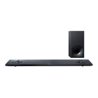
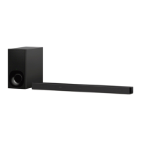
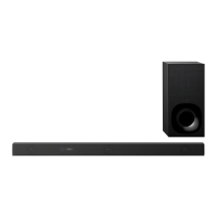
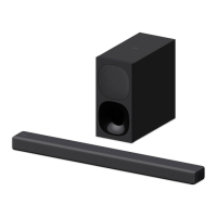
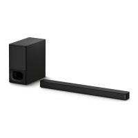
HT-NT3
68
Pin No. Pin Name I/O Description
F1 VDDQ - DQ Power Supply: 1.5V +/-0.075V
F2 DQL2 I/O Data Input/output: Bi-directional data bus.
F3 DQSL I/O
Data Strobe: Output with read data, input with write data. Edge-aligned with read data, cen-
tered in write data. For the x16, DQSL: corresponds to the data on DQL0-DQL7; DQSU corre-
sponds to the data on DQU0-DQU7. The data strobe DQS, DQSL and DQSU are paired with
differential signals DQS, DQSL and DQSU, respectively, to provide differential pair signaling to
the system during reads and writes. DDR3 SDRAM supports differential data strobe only and
does not support single-ended.
F4 NO_USE - Not used
F5 NO_USE - Not used
F6 NO_USE - Not used
F7 DQL1 I/O Data Input/output: Bi-directional data bus.
F8 DQL3 I/O Data Input/output: Bi-directional data bus.
F9 VSSQ - DQ Ground
G1 VSSQ - DQ Ground
G2 DQL6 I/O Data Input/output: Bi-directional data bus.
G3
DQSL I/O
Data Strobe: Output with read data, input with write data. Edge-aligned with read data, cen-
tered in write data. For the x16, DQSL: corresponds to the data on DQL0-DQL7; DQSU corre-
sponds to the data on DQU0-DQU7. The data strobe DQS, DQSL and DQSU are paired with
differential signals DQS, DQSL and DQSU, respectively, to provide differential pair signaling to
the system during reads and writes. DDR3 SDRAM supports differential data strobe only and
does not support single-ended.
G4 NO_USE - Not used
G5 NO_USE - Not used
G6 NO_USE - Not used
G7 VDD - Power Supply: 1.5V +/-0.075
G8 VSS - Ground
G9 VSSQ - DQ Ground
H1 VREFDQ - Reference voltage for DQ
H2 VDDQ - DQ Power Supply: 1.5V +/-0.075V
H3 DQL4 I/O Data Input/output: Bi-directional data bus.
H4 NO_USE - Not used
H5 NO_USE - Not used
H6 NO_USE - Not used
H7 DQL7 I/O Data Input/output: Bi-directional data bus.
H8 DQL5 I/O Data Input/output: Bi-directional data bus.
H9 VDDQ - DQ Power Supply: 1.5V +/-0.075V
J1 NC - No Connect: No internal electrical connection is present.
J2 VSS - Ground
J3
RAS I Command Input: RAS (along with CS) defi ne the command being entered.
J4 NO_USE - Not used
J5 NO_USE - Not used
J6 NO_USE - Not used
J7 CK I
Clock: CK is differential clock input. All address and control input signals are sampled on the
crossing of the positive edge of CK. Output (read) data is referenced to the crossing of CK.
J8 VSS - Ground
J9 NC - No Connect: No internal electrical connection is present.
K1 ODT I
On Die Termination: ODT (registered HIGH) enables termination resistance internal to the
DDR3 SDRAM. When enabled, ODT is only applied to each DQ, DQS, DQS and DM/TDQS,
NU/TDQS (When TDQS is enabled via Mode Register A11=1 in MR1) signal for x8 confi gura-
tions. The ODT pin will be ignored if the Mode Register (MR1) is programmed to disable ODT.
K2 VDD - Power Supply: 1.5V +/-0.075
K3
CAS I Command Input: CAS (along with CS) defi ne the command being entered.
K4 NO_USE - Not used
K5 NO_USE - Not used
K6 NO_USE - Not used
K7
CK I
Clock: CK is differential clock input. All address and control input signals are sampled on the
crossing of the negative edge of CK. Output (read) data is referenced to the crossing of CK.
K8 VDD - Power Supply: 1.5V +/-0.075
 Loading...