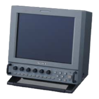
5-13
• MA-324 (H) BOARD IC302 CXA3106Q-T6 (PLL)
Pin No. Pin Name I/O Description
1 IOVCC —
Power supply terminal (+5V) (digital system)
2 IOGND —
Ground terminal (digital system)
3 VCOH I
External VCO input terminal Not used (open)
4VCOLI
External inverted VCO input terminal Not used (open)
5 VCO I
External VCO input terminal Not used (open)
6HOLDI
Phase comparison disable signal input terminal Not used (fixed at “L”)
7 SYNCH I
Sync signal input terminal Not used (open)
8 SYNCL I
Inverted sync signal input terminal Not used (open)
9SYNCI
Horizontal sync signal input terminal
10 SENABLE I
Enable signal input from the system controller (IC501)
11 SCLK I
Serial data transfer clock signal input from the system controller (IC501)
12 SDATA I
Serial data input from the system controller (IC501)
13 TLOAD I
Programmable counter test input terminal Not used (fixed at “H”)
14 CS I
Chip select signal input terminal Not used (fixed at “H”)
15 SEROUT O
Register read output terminal Not used (open)
16 DIVOUT O
Programmable counter test output terminal Not used (open)
17 UNLOCK O
Unlock signal output terminal Not used (open)
18 DVCC —
Power supply terminal (+5V) (digital system)
19 DGND —
Ground terminal (digital system)
20 CLK/2N O
Inverted 1/2 clock signal output terminal Not used (open)
21 CLK/2 O
1/2 clock signal output terminal Not used (open)
22 CLKN O
Inverted clock signal output terminal Not used (open)
23 CLK O
Clock signal output to the LCD timing generator (IC301) and on screen display controller
(IC401)
24 DSYNC O
Delay sync signal output to the LCD timing generator (IC301)
25 TTLGND —
Ground terminal (for TTL output)
26 TTLVCC —
Power supply terminal (+5V) (for TTL output)
27 IOGND —
Ground terminal (digital system)
28 PECLVCC —
Power supply terminal (+5V) (for PECL output)
29 CLK/2L O
Inverted 1/2 clock signal output terminal Not used (pull-up)
30 CLK/2H O
1/2 clock signal output terminal Not used (pull-up)
31 CLKL O
Inverted clock signal output to the LCD drive IC (IC202 to 204)
32 CLKH O
Clock signal output to the LCD drive IC (IC202 to 204)
33 DSYNCL O
Delay sync signal output terminal Not used (pull-up)
34 DSYNCH O
Inverted delay sync signal output terminal Not used (pull-up)
35 VBB O
Reference voltage output for the PECL Not used (open)
36 PECLVCC —
Power supply terminal (+5V) (for PECL output)
37 IOGND —
Ground terminal (digital system)
38 IOVCC —
Power supply terminal (+5V) (digital system)
39 PLLVCC —
Power supply terminal (+5V) (for PLL circuit/analog system)
40 PLLGND —
Ground terminal (for PLL circuit/analog system)
41 VCOVCC —
Power supply terminal (+5V) (for VCO circuit/analog system)
42 VCOGND —
Ground terminal (for VCO circuit/analog system)
43 VCOHGND —
Ground terminal (for VCO sub/analog system)
44 IREF —
Charge pump current generating terminal
45 RC2 —
Connection terminal of low-pass filter for the charge pump
w
w
w
.
x
i
a
o
y
u
1
6
3
.
c
o
m
Q
Q
3
7
6
3
1
5
1
5
0
9
9
2
8
9
4
2
9
8
T
E
L
1
3
9
4
2
2
9
6
5
1
3
9
9
2
8
9
4
2
9
8
0
5
1
5
1
3
6
7
3
Q
Q
TEL 13942296513 QQ 376315150 892498299
TEL 13942296513 QQ 376315150 892498299
http://www.xiaoyu163.com
http://www.xiaoyu163.com