5-16
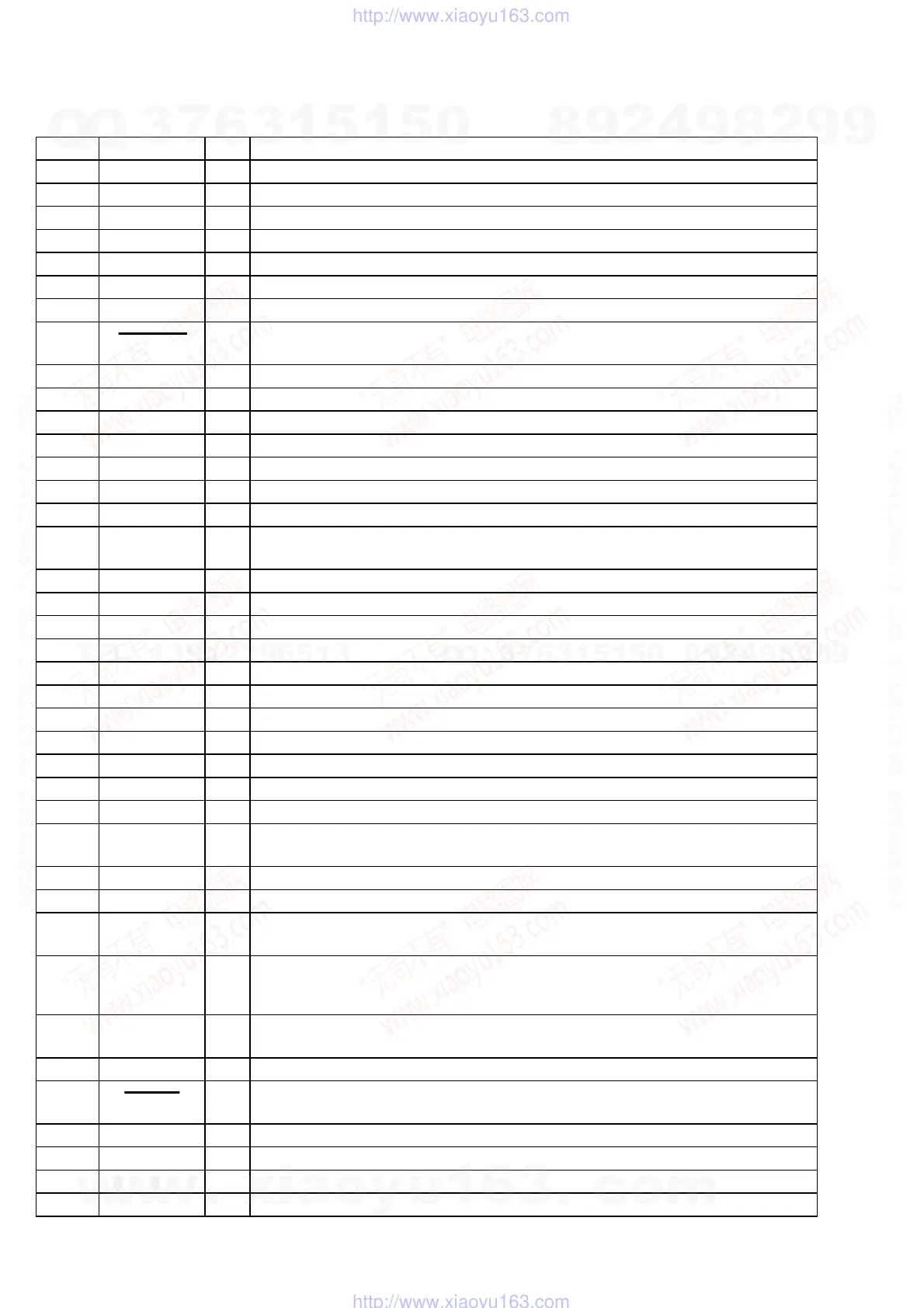
• MA-324 (H) BOARD IC501 S579193PZ-TEB (SYSTEM CONTROLLER)
Pin No. Pin Name I/O Description
1 LANC IN I
LANC data input for adjustment
2 LANC OUT O
LANC data output for adjustment
3 XS CONT O
Video selection signal output terminal “L”: S terminal, “H”: composite Not used (open)
4—O
Not used (open)
5 IIC SDA I/O
Two-way data bus with the gamma control IC (IC201)
6 IIC SCL O
Shift clock signal output to the gamma control IC (IC201)
7, 8 — O
Not used (open)
9 XSYS RES O
Reset signal output to the D/A converter (IC207), on screen display controller (IC401), etc.
“L”: reset
10 to 12 — O
Not used (open)
13 VSS —
Ground terminal
14 XPOWER SW I
Power (on/off) switch (S902) input terminal “L” active
15 XENTER I
Jog dial click input from rotary encoder (S905) for the menu setting “L” active
16 XMENU I
Menu selection (menu on/off) switch (S903) input terminal “L” active
17 XPASS RES I
Password reset switch (S501) input terminal “L” active
18 VIDEO/XPC IN I
Input selection (video/PC) switch (S904) input terminal “L”: PC, “H”: video
19
PC/XV AU
CONT
O
Control signal output to the sync signal select switch (IC132, 133) “L”: video, “H”: PC
20
EXT 3D CONT
O
External 3D control signal output terminal “H” active
21
SHUTTER MUTE
O
Shutter wave mute control signal output terminal “H”: mute on
22 XCS TG O
Chip select signal output to the LCD timing generator (IC301) “L” active
23 XCS PLL O
Chip select signal output to the PLL (IC302) “L” active
24 XCS DA5 O
Chip select signal output to the D/A converter (IC205, 206) “L” active
25 XCS DA12 O
Chip select signal output to the D/A converter (IC207) “L” active
26 XCS EEPROM O
Chip select signal output to the EEPROM (IC502) “L” active
27 XEEPROM WE O
Data write enable signal output to the EEPROM (IC502) “L” active
28 XCS DAYC O
Chip select signal output to the D/A converter (IC507) “L” active
29 P SAVE LED O
LED drive signal output of the POWER SAVING indicator (D901-2 (red)) “H”: LED on
30 3D POL IN I
POLARITY switch (S901) input terminal “L”: B, “H”: A
31 HSYNC2 I
Horizontal sync signal (external event) input terminal
Horizontal sync signal frequency is divided, then input
32 L/R FLD I
L/R field inverted signal (frame control pulse) detection terminal
33 HI SI I
Serial data input from the EEPROM (IC502)
34 HI SO O
Serial data output to the D/A converter (IC205 to 207), LCD timing generator (IC301), PLL
(IC302), on screen display controller (IC401), EEPROM (IC502) and D/A converter (IC507)
35 XHI SCK O
Serial data transfer clock signal output to the D/A converter (IC205 to 207), LCD timing
generator (IC301), PLL (IC302), on screen display controller (IC401), EEPROM (IC502) and
D/A converter (IC507)
36 SHUTTER O
Shutter wave (500 Hz rectangular wave) output terminal
Frequency is divided into 4 externally
37 — O
Not used (open)
38 XRESET I
System reset signal input from the reset signal generator (IC504) “L”: reset
For several hundreds msec. after the power supply rises, “L” is input, then it changes to “H”
39 VSS —
Ground terminal
40 20MHZ OUT O
Main system clock output terminal (20 MHz)
41 20MHZ IN I
Main system clock input terminal (20 MHz)
42 VDD —
Power supply terminal (+5V)
w
w
w
.
x
i
a
o
y
u
1
6
3
.
c
o
m
Q
Q
3
7
6
3
1
5
1
5
0
9
9
2
8
9
4
2
9
8
T
E
L
1
3
9
4
2
2
9
6
5
1
3
9
9
2
8
9
4
2
9
8
0
5
1
5
1
3
6
7
3
Q
Q
TEL 13942296513 QQ 376315150 892498299
TEL 13942296513 QQ 376315150 892498299
http://www.xiaoyu163.com
http://www.xiaoyu163.com