5-15
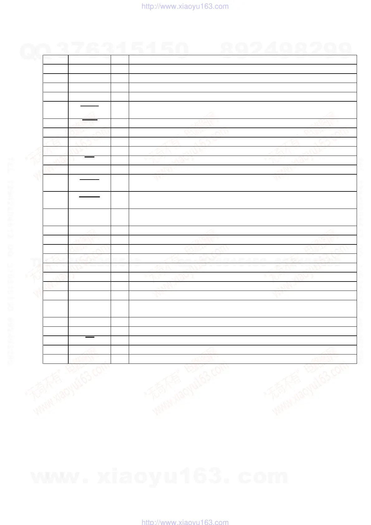
• MA-324 (H) BOARD IC401 MB90096PF-G-150-BND (ON SCREEN DISPLAY CONTROLLER)
Pin No. Pin Name I/O Description
1 CPOUT O
Horizontal sync phase comparison result output terminal Not used (open)
2 AVSS1 —
Ground terminal (for internal VCO)
3 VCOIN I
Internal VCO voltage input terminal Not used (fixed at “L”)
4 AVSS2 —
Ground terminal (for internal VCO)
5 RESET I
System reset signal input from the system controller (IC501) “L”: reset
For several hundreds msec. after the power supply rises, “L” is input, then it changes to “H”
6 TEST I
Input terminal for the test Not used (fixed at “H”)
7 VSS —
Ground terminal
8 DOCKI I
Dot clock signal input from the PLL (IC302)
9 DOCKO O
Dot clock signal output terminal Not used (open)
10 FH O
Output terminal of horizontal sync signal generated in PLL circuit Not used (open)
11 EVEN I
Field control signal input terminal Not used (fixed at “H”)
12 HSYNC I
Horizontal sync signal input from the LCD timing generator (IC301)
Based in this signal period, dot clock signal is generated Active level is programmable
13 VSYNC I
Vertical sync signal input from the LCD timing generator (IC301)
Active level is programmable
14 DISP I
Display outputs (ROUT, GOUT, BOUT, IOUT, VOB1, VOB2) control signal input from the
system controller (IC501)
15 VOB2 O
Semi-transparent period output terminal Active level is programmable Not used (open)
16 VOB1 O
OSD display period output terminal Active level is programmable
17 IOUT (C3) O
Color signal (I) output terminal Active level is programmable Not used (open)
18 GOUT (C2) O
Color signal (G) output terminal Active level is programmable
19 ROUT (C1) O
Color signal (R) output terminal Active level is programmable
20 BOUT (C0) O
Color signal (B) output terminal Active level is programmable
21 V3V —
Coupling capacitor connection terminal
22 VCC —
Power supply terminal (+5V)
23 TRE O
Output of signal indicating that the command is being transferred to system controller (IC501)
and the fill operation is under way “H” active
24 SCLK I
Serial data transfer clock signal input from the system controller (IC501)
25 SIN I
Serial data input from the system controller (IC501)
26 CS I
Chip select signal input from the system controller (IC501) “L” active
27 AVCC —
Power supply terminal (+5V) (for internal VCO)
28 AV3V —
Coupling capacitor connection terminal
w
w
w
.
x
i
a
o
y
u
1
6
3
.
c
o
m
Q
Q
3
7
6
3
1
5
1
5
0
9
9
2
8
9
4
2
9
8
T
E
L
1
3
9
4
2
2
9
6
5
1
3
9
9
2
8
9
4
2
9
8
0
5
1
5
1
3
6
7
3
Q
Q
TEL 13942296513 QQ 376315150 892498299
TEL 13942296513 QQ 376315150 892498299
http://www.xiaoyu163.com
http://www.xiaoyu163.com