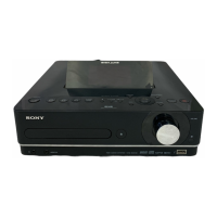
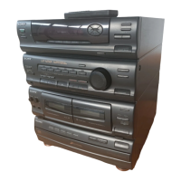
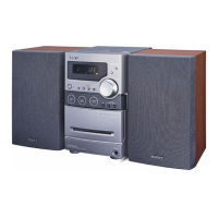
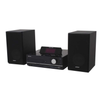
NAS-E35HD/SS-CE35HD
NAS-E35HD/SS-CE35HD
2525
For Schematic Diagrams.
Note:
• All capacitors are in μF unless otherwise noted. (p: pF) 50
WV or less are not indicated except for electrolytics and
tantalums.
• All resistors are in Ω and 1/4 W or less unless otherwise
specifi ed.
•
f
: internal component.
• 2 : nonfl ammable resistor.
• C : panel designation.
THIS NOTE IS COMMON FOR PRINTED WIRING BOARDS AND SCHEMATIC DIAGRAMS.
(In addition to this, the necessary note is printed in each block.)
• A : B+ Line.
• Voltages and waveforms are dc with respect to ground
under no-signal conditions.
– CD Board –
no mark
: CD PLAY
– USB MICOM Board –
no mark
: USB PLAY
– Other Boards –
no mark
: TUNER (FM/AM)
( ) : CD PLAY
‹‹ ›› : USB PLAY
• Voltages are taken with VOM (Input impedance 10 MΩ).
• Circled numbers refer to waveforms.
• Signal path.
F : TUNER (FM/AM)
J : CD PLAY
i : AUDIO IN
f : HDD
d : DAB
a : USB
l : DMPORT
• Abbreviation
AR : Argentina model
AUS : Australian model
E51 : Chilean and Peruvian models
MX : Mexican model
RU : Russian model
For Printed Wiring Boards.
Note:
• X : Parts extracted from the component side.
• Y : parts extracted from the conductor side.
•
f
: internal component.
• : Pattern from the side which enables seeing.
(The other layers' patterns are not indicated.)
• Indication of transistor.
These are omitted.
These are omitted.
Caution:
Pattern face side:
(SIDE B)
Parts face side:
(SIDE A)
Parts on the pattern face side seen from
the pattern face are indicated.
Parts on the parts face side seen from
the parts face are indicated.
Note: The components identifi ed by mark 0 or dotted
line with mark 0 are critical for safety.
Replace only with part number specifi ed.
Caution:
Pattern face side:
(Conductor Side)
Parts face side:
(Component Side)
Parts on the pattern face side seen from
the pattern face are indicated.
Parts on the parts face side seen from
the parts face are indicated.
• USB MICOM board is multi-layer printed board.
However, the patterns of intermediate-layers have not
been included in diagrams.
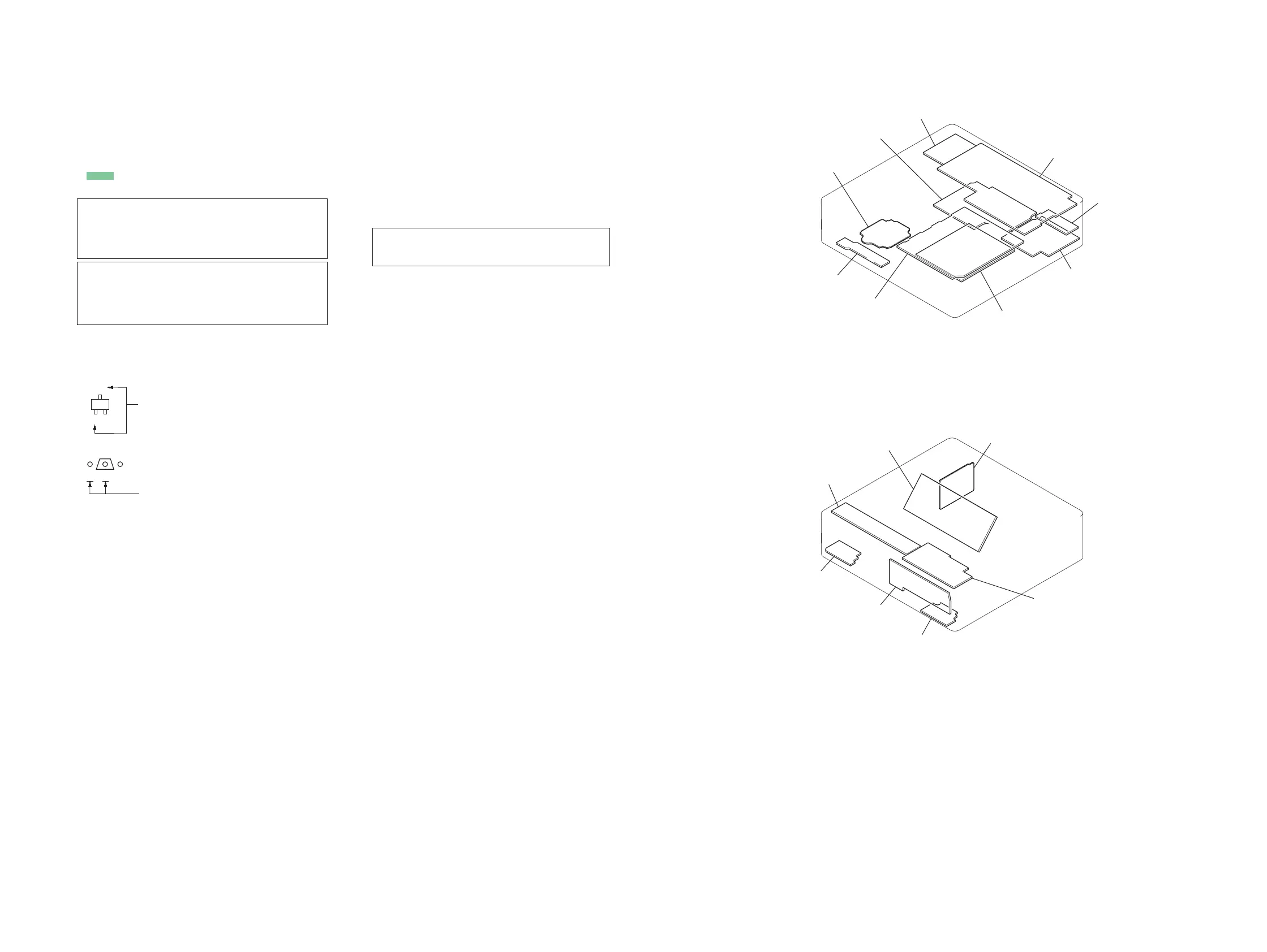
• Circuit Boards Location