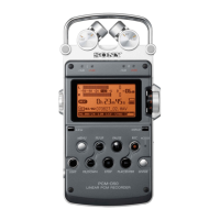
PCM-D50
57
Pin No.Pin NameI/O Description
R19 GND — Ground
R22, R23LCD_R2, LCD_R4_ — Not used (Open)
R24 GNDSINK — Ground
R25 VDD_L0 — Power supply (VDD_L0)
R26 VUSB — Not used (Open)
T1 SDR_CKE0OClock enable signal output to SD-RAM
T2 SDR_CSZ1OChip select signal output (Not used in this set) (Open)
T3 SDR_CSZ0OChip select signal output to SD-RAM
T4 SDR_BA1OBank address signal output to SD-RAM
T5 SDR_RASZORow address strobe signal output to SD-RAM
T8 SDR_CKE1OClock enable signal output to SD-RAM (Not used in this set) (Open)
T9 GND — Ground
T10 MWI_SO — Not used (Open)
T17, T18U70_SOUT, U70_SRIN — Not used (Open)
T19 GND — Ground
T22 LCD_R5 — Not used (Open)
T23 VUSBIN — Not used (Open)
T24 C_TMS — Not used (Open)
T25 VLOG ONot used (Open)
T26 CKO OMain system clock output (12MHz)
U1 to U5SDR_A12 to SDR_A8OAddress signal output to SD-RAM
U8 SDR_CASZOColumn address strobe signal output to SD-RAM
U9 GND — Ground
U10 MWI_CSZ0 — Not used (Open)
U11 MWI_SK — Not used (Open)
U12, U13GIO_P1, GIOP0 — Not used (Open)
U14 L0_DET — Not used (Open)
U15 L1_DET — Connected to V16 pin
U16ERR_RST_REQZINot used (Pull up)
U17 CK32KI I32kHz clock input (Not used in this set) (Open)
U18 REFCLKOOMaster clock signal output (Not used in this set) (Open)
U19 D_TCK OLCD reset signal output
U22 C_TDO — Not used (Open)
U23 VLOGIN — Power supply (+3.3V)
U24 C_TCK — Not used (Open)
U25 VPLL OVDD_PLL Power supply output
U26 CKI IMain system clock input (12MHz)
V1 to V3 IO_A — Power supply (VDD_IOA)
V4, V5, V8
SDR_A6, SDR_A5,
SDR_A7
OAddress signal output to SD-RAM
V9 GND — Ground
V10 SPI1_SKOSerial clock signal output to the digital audio I/F transceiver
V11 MWI_CSZ1 — Ground
V12 to V15GND — Ground
V16 DSP_DET — Connected to U15 pin
V17 D_TMS IMIC L/R direction switch signal input
V18 D_TDO OPOWER ON control signal output
V19 D_TRSTZIInterrupt signal input from the digital audio I/F transceiver
V22 C_RTCK — Not used (Open)
V23 C_TRSTZ — Not used (Open)
V24 VPLLIN — Power supply (+3.3V)
V25 VDSPIN — Power supply (+3.3V)
V26 VDSP — Not used (Open)
W1 IOGND — Ground
W2 GPIO14 IEXT MIC connection detection signal input
W3 GPIO15 IMS-INS signal input
WWW.OURDEV.CN
 Loading...