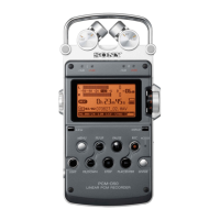
PCM-D50
58
Pin No.Pin NameI/O Description
W4, W5SDR_A4, SDR_A3OAddress signal output to SD-RAM
W8 SPI1_SOOSerial data output to the digital audio I/F transceiver
W9 GND — Ground
W10SPI1_CSZ0OChip select signal output to the digital audio I/F transceiver
W11 toW18
GND — Ground
W19EXTPCMCLKIMCLK clock input
W22 D_TDI OCD signal output to the LCD unit
W23 C_TDI — Not used (Open)
W24, W25 IO_B — Power supply (VDD_GP1)
W26 VLO OVDD_L0 power supply output
Y1 IOVDD — Power supply (VDD_GP1)
Y2 GPIO13 IHeadphone connection detection signal input
Y3 GPIO12 IPOWER (S2002) switch off signal input
Y4, Y5SDR_A2, SDR_A1OAddress signal output to SD-RAM
Y22, Y23TM1, TM0INot used (Pull up)
Y24, Y25VDD_DSP — Power supply (VDD_L1)
Y26 VHP — Not used (Open)
AA1 GPIO12 ISIRCS detect signal input
AA2 GPIO10 ILOW CUT FILTER (S1602) switch signal input
AA3 GPIO9 ILIMITER (S1601) switch signal input
AA4 SDR_A0OAddress signal output to SD-RAM
AA5 SDR_CLKOClock signal output to SD-RAM
AA22,AA23
TMC2, TMG — Not used (Connected ground)
AA24 TM2 INot used (Pull up)
AA25 VANAIN — Power supply (+3.3V)
AA26 VANA OVDD_ANA power supply output
AB1 VDD_L0 — Power supply (VDD_L0)
AB2 GPIO8 IDPC (S2213) switch signal input
AB3 GPIO7 IUSB interrupt signal input
AB4 GPIO6 ILINE IN connection detection signal input
AB5 SDR_BA0OBank address signal output to SD-RAM
AB6SPI0_CSZ1 — Not used (Connected ground)
AB7 SPI0_SI INot used (Open)
AB8 SPI1_SI ISerial data input from the digital audio I/F transceiver
AB9 IO_C — Power supply (VDD_GP1)
AB10CAM_YUV7OMIC/LINE IN power supply control signal output
AB11CAM_YUV4OPower supply control signal output
AB12CAM_CLKOLINE IN (OPT) receiver power control signal output
AB13CAM_STRO24.575MHz clock generator control signal output
AB14CAM_SCLKODIV clock control signal output
AB15 to
AB17
MS_DATA3, MS_DATA2,
MS_DATA0
I/OMS data input/output
AB18 MS_INSZIRead/busy signal input
AB19 EXTCLK — Not used (Open)
AB20PM1_SENOL/R sampling clock signal output to the D/A converter
AB21 PM1_CLKOSerial clock signal output to the D/A converter
AB22PM0_SENOL/R sampling clock signal output to the D/A converter
AB23, AB24
TCM1, TM3 — Not used (Connected ground)
AB25 GND1 — Ground
AB26 OSCIN ISub system clock input (32.768kHz)
AC1 toAC3
IO_A — Power supply (VDD_IOA)
AC4 GPIO5 ILINE IN (OPT) connection detection signal input
AC5 GPIO4 ILINE OUT connection detection signal input
AC6SPI0_CSZ0OChip select signal output to the LCD unit
AC7 SPI0_SKOSerial data transfer clock signal output to the D/A converter
AC8 SPI0_SOOSerial date output to the LCD unit
WWW.OURDEV.CN
 Loading...