2020
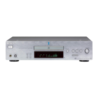
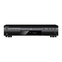
SCD-CE595
SCD-CE595
• IC Pin Function Description
• MAIN BOARD IC705 HD6432238RN51TEV (SYSTEM CONTROLLER)
• IC Block Diagrams
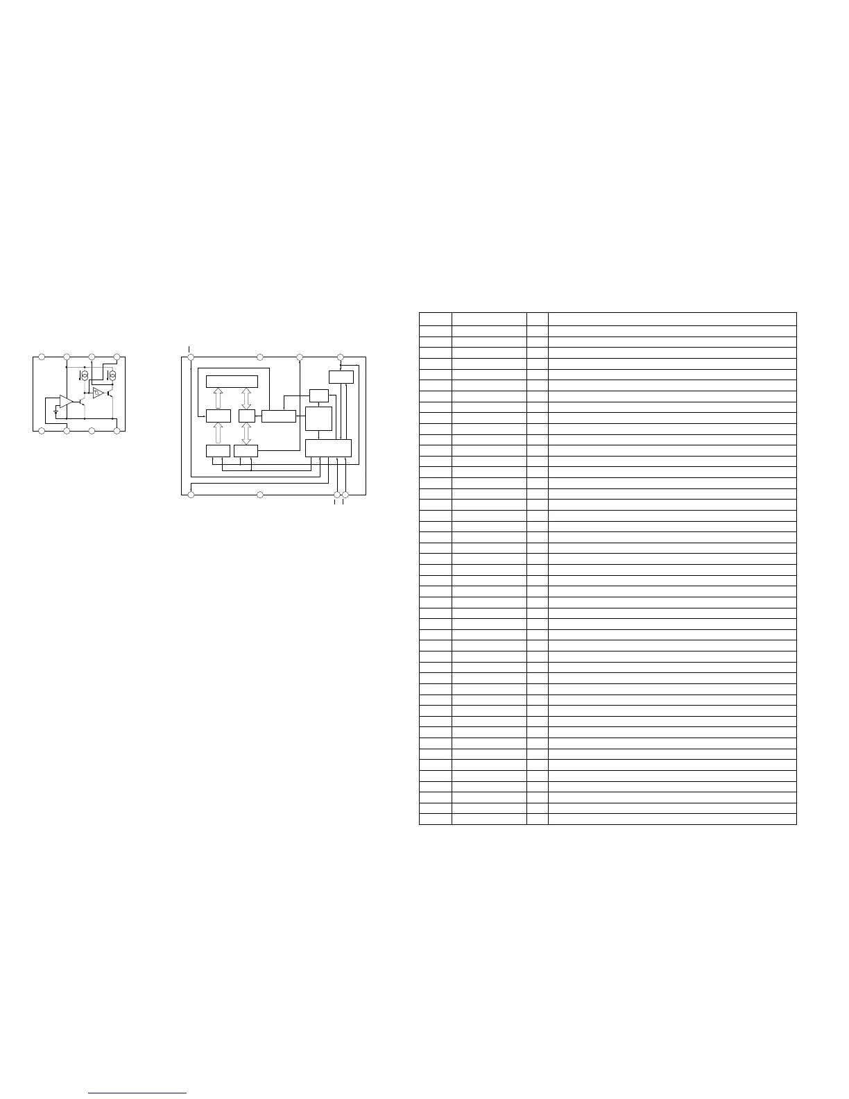
IC701 M51957BFP-600C
+
–
3
4
NC
IN
NC
GND
NC
VCC
OUT
C
1.25V
1
7
6
5
8
2
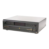
IC702 BR9040F-WF2
8 7 6 5
1 2 3 4
DI
DO
GND
WC
SK
CS
VCC
R/B
COMMAND DECODE
CONTROL CLOCK
GENERATION
POWER
SUPPLY
VOLTAGE
DETECTOR
HIGH VOLTAGE
GENERATOR
WRITE
DISABLE
COMMAND
REGISTER
ADDRESS
BUFFER
DATA
REGISTER
ADDRESS
DECODER
R/W
AMP
4096bit
EEPROM ARRAY
8bit
16bit
16bit
8bit
– MAIN Board –
Pin No. Pin Name I/O Description
1SDATA DAC O Data output to the DAC (IC200)
2 SCLK DAC O Clock output to the DAC (IC200)
3 SLATR DAC O Latch (R-ch) output to the DAC (IC200)
4 to 11 CD0 to 7 I/0 Data Bus to the Digital Servo Processor (IC706)
12 CVCC — Power supply terminal (+3.3V)
13 CA0 O Address Bus to the Digital Servo Processor (IC706)
14 VSS — Ground terminal
15 to 22 CA1 to 8 O Address Bus to the Digital Servo Processor (IC706)
23 PB1 — Not used (open)
24 PB2 — Not used (open)
25 LOAD S0 I DISK cyacking select (SO)
26 LOAD S1 I TRAY (S2:OPEN)
27 LOAD S2 I TRAY (S1:TURN)
28 TSENS I T sens signal input
29 DSENS I DISK sens signal input
30 TRAY IN O TRAY in control output to the Motor Driver (IC712)
31 RS232CTX O PC serial signal
32 RS232CRX I PC serial signal
33 TRAY OUT O TRAY out control output to the Motor Driver (IC712)
34 P10 — Not used (open)
35 DRV ON O Driver mute output to the Motor Driver (IC712)
36 SP ON O Spindle mute output to the Motor Driver (IC712)
37 P13 — Not used (open)
38 XLDON O LD ON/OFF output to the Motor Driver (IC712)
39 TRMP O Table control (+Clockwise) output to the TMD (IC710)
40 TRMM O Table control (-Counterclock) output to the TMD (IC710)
41 P17 — Not used (open)
42 AVSS — Ground terminal
43 DIAO I Test Mode input
44 P96 — Ground terminal
45 to 50 P47 to P42 — Ground terminal
51 MODEL I Model check (L:1Hi,Mi:5Es,H:5 Hi)
52 JIT I Waltz jetter select
53 VREF I Reference voltage
54 AVCC — Power supply terminal (+3.3V)
55 MD0 I Muving mode control 0
56 MD1 I Muving mode control 1
57 OSC2 — Not used (open)
58 OSC1 — Ground terminal
59 XRST O System reset
60 XNMI I NMI input (fixed at “H”)
61 XSTBY I Standby input (fixed at “H”)
62 VCC — Power supply terminal (+3.3V)
63 XTAL — Not used (open)
64 VSS1 — Ground terminal
65 EXTAL I External clock input