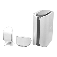
SA-WSF200/WSF500/SS-CTF500/F500/TSF200/TSF500
31
• IC Pin Function Description
AMP-DSP BOARD (SA-WSF200/WSF500) IC611 R5F3640DDFAR (SA-WSF200), R5F3640MDFAR (SA-WSF500)
(SYSTEM CONTROLLER)
Pin No. Pin Name I/O Description
1 DAMP_SCDT/DIR_DIN O Serial data output to the digital audio interface receiver and stream processor
2
DAMP_SHIFT/
DIR_CLK
O Shift clock signal output to the digital audio interface receiver and stream processor
3 DSP_INT I Interrupt signal input from the DSP
4 - - Not used
5 DSP_MOSI O Serial data output to the DSP
6 DSP_MISO I Serial data input from the DSP
7 DSP_SPICLK O Serial data transfer clock signal output to the DSP
8 BYTE I External data bus width selection signal input terminal Fixed at "L" in this set
9 CNVSS I Processor mode switch input terminal Not used
10, 11 - - Not used
12 RESET I
System reset signal input from the reset signal generator "L": reset
For several hundreds msec. after the power supply rises, "L" is input, then it change to "H"
13 XOUT O Main system clock output terminal (10 MHz)
14 VSS - Ground terminal
15 XIN I Main system clock input terminal (10 MHz)
16 VCC1 - Power supply terminal (+3.3V)
17 NMI I Non-maskable interrupt input terminal Fixed at "H" in this set
18 DIR_ZERO I Audio serial data input from the digital audio interface receiver
19 DIR_CSFLAG I CSFLAG data input from the digital audio interface receiver
20 AC_CUT I AC cut detection signal input terminal "L": AC cut on
21 to 26 - - Not used
27 DIR_ERROR I Error signal input from the digital audio interface receiver
28 P_CONT_FL O Power on/off control signal output terminal "H": power on
29 IIC_CLK I/O Two-way I2C clock bus terminal Not used
30 IIC_DATA I/O Two-way I2C data bus terminal Not used
31 SYS_TXD O Serial data output to the SYSTEM CONTROL connector (HCD-F200/F500)
32 SYS_RXD I Serial data input from the SYSTEM CONTROL connector (HCD-F200/F500)
33 SYS_CLK I
Serial data transfer clock signal input from the SYSTEM CONTROL connector
(HCD-F200/F500)
34 SYS_BUSY O Busy signal output to the SYSTEM CONTROL connector (HCD-F200/F500)
35 EEPROM_SDA I/O I2C Two-way data bus with the EEPROM
36 EEPROM_SCL I/O I2C data transfer clock signal input/output with the EEPROM
37, 38 - - Not used
39, 40
P_CONT_PVDD,
P_CONT1
O Power on/off control signal output terminal "H": power on
41 EPM I Not used
42 to 44 - - Not used
45 P_CONT_DSP O Power on/off control signal output terminal for the DSP "H": power on
46 CE I Chip enable signal input terminal Not used
47 DAMP_INIT O Reset signal output to the stream processor "L": reset
48 DAMP_SOFT_MUTE O Soft muting on/off control signal output to the stream processor "L": muting on
49, 50
DAMP_LATCH1,
DAMP_LATCH3
O Serial data latch pulse signal output to the stream processor
51 DRIVE_RST (EN) O Reset signal output to the digital power amplifi er "L": reset
52 - - Not used
53, 54
OVERFLOW1,
OVERFLOW2
I Over fl ow status input from the stream processor
55 DSP_RESET O Reset signal output to the DSP "L": reset
56 DSP_SPIDS O Device selection signal output to the DSP
57 DIR_RST O Reset signal output to the digital audio interface receiver "L": reset
58 DIR_HCE O Chip enable signal output to the digital audio interface receiver
59 OVERFLOW3 I Over fl ow status input terminal Not used
60 DIR_XSTATE I Source clock selection monitor input from the digital audio interface receiver
61 - - Not used
62 VCC2 - Power supply terminal (+3.3V)
63 - - Not used
 Loading...