146
STR-DA5200ES
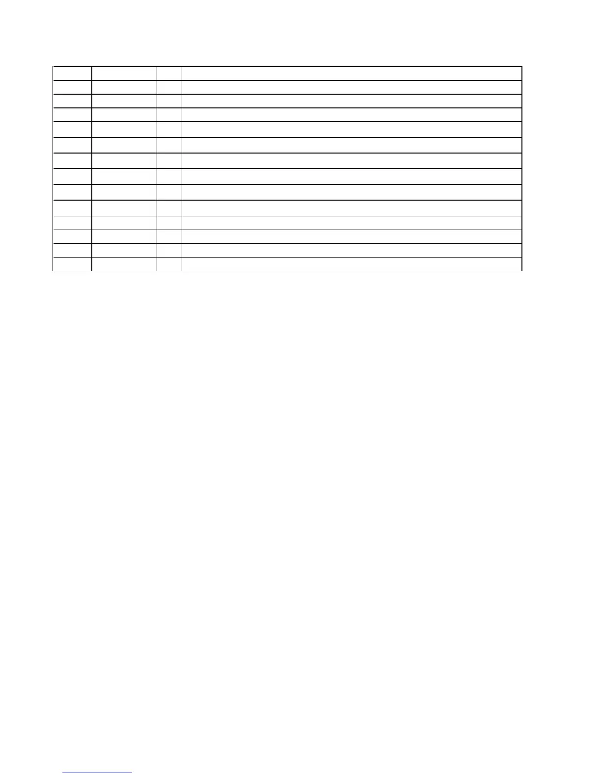
Pin No.
Pin Name I/O Description
79
UHC124_RST O Reset signal output to the DSP
80
NC - Not used
81
DVCC - Power supply terminal (+3.3 V)
82 RD O
Read strobe signal output to the USB interface and FCRAM
83 SRWR O
Write strobe signal output to the USB interface and FCRAM
84 SRLLB O
Upper byte column address strobe signal output to the FCRAM
85 SRLUB O
Lower byte column address strobe signal output to the FCRAM
86
LRCK O L/R sampling block signal (44.1KHz) output to the DSP
87 BCK O
Bit clock signal (2.8224 MHz) output to the DSP
88
DVSS - Ground terminal
89 to 91
PC3 to PC1 - Not used
92
PC0 (REQ) O Request signal output to the DSP
93 to 100
PG7 to PG0 - Not used

 Loading...