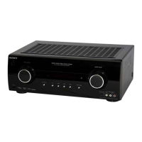
Do you have a question about the Sony STR-KM2 and is the answer not in the manual?
Details the power output and impedance for various audio modes.
Lists analog and digital input types and their characteristics.
Details the analog audio output voltage and impedance.
Provides tuning range and antenna connection specifications.
Details power input voltage and frequency requirements by region.
Guidelines for replacing chip components, including notes on tantalum capacitors and unleaded solder.
Visual flowchart outlining the sequence for disassembling the set.
Detailed steps and diagrams for removing the unit's outer case.
Detailed steps and diagrams for removing the front panel assembly.
Detailed steps and diagrams for removing the back panel assembly.
Procedure for disassembling the main internal block components.
Procedure for removing the main and thermal boards, including solder desoldering.
Tests all fluorescent display segments by cycling through them.
Displays software versions for microprocessor, DSP firmware, sound tuning, and tuner.
Tests FM tuner auto-stop functionality using a signal generator.
Block diagram illustrating the signal flow within the tuner and audio processing sections.
Block diagram detailing the signal paths within the digital processing and interface sections.
Block diagram showing the signal flow for HDMI input and output processing.
Block diagram illustrating the functions of the key input, display driver, and USB interface circuits.
Block diagram showing the power control, amplifier drive, and protection circuits.
Component layout for the DIGITAL AUDIO board, Side A.
Component layout for the DIGITAL AUDIO board, Side B.
Circuit schematic for the DIGITAL AUDIO board, part 1 of 4.
Circuit schematic for the DIGITAL AUDIO board, part 2 of 4.
Circuit schematic for the DIGITAL AUDIO board, part 3 of 4.
Circuit schematic for the DIGITAL AUDIO board, part 4 of 4.
Component layout for the MAIN board.
Circuit schematic for the MAIN board, part 1 of 4.
Circuit schematic for the MAIN board, part 2 of 4.
Circuit schematic for the MAIN board, part 3 of 4.
Circuit schematic for the MAIN board, part 4 of 4.
Component layout for the HDMI RE board, Side A (KM3).
Component layout for the HDMI RE board, Side B (KM3).
Circuit schematic for the HDMI RE board, part 1 of 2 (KM3).
Circuit schematic for the HDMI RE board, part 2 of 2 (KM3).
Component layout for the POWER AVIDEO board.
Circuit schematic for the POWER AVIDEO board.
Component layout for the DISPLAY board.
Circuit schematic for the DISPLAY board.
Component layout for the DCDC board.
Circuit schematic for the DCDC board.
Component layout for the LED BAR board.
Circuit diagram for the LED BAR board, showing component connections and functions.
Component layout for the USB board (excluding SAF, AR models).
Circuit schematic for the USB board (excluding SAF, AR models).
Component layout for the TUNER1 board.
Circuit diagram for the TUNER1 board, detailing tuner and audio interface components.
Component layout for the POWER KEY board.
Circuit diagram for the POWER KEY board, illustrating button and LED connections.
Component layout for the thermal board, showing sensor and connector placement.
Circuit diagram for the thermal board, detailing sensor and power connections.
Block diagram and pinout for the WM8768GEDS/R IC on the DIGITAL AUDIO board.
Detailed descriptions of IC pin functions for various components.
Exploded view showing the main chassis, front panel, and back panel components.
Exploded view detailing the components of the front panel assembly.
Exploded view detailing the components of the back panel assembly.
Exploded view showing the main chassis and heatsink assembly components.
| Type | AV receiver |
|---|---|
| Channels | 5.1 |
| Surround Sound Formats | Dolby Digital, DTS |
| Inputs | 2 x audio |
| Outputs | 1 x Video (Composite), 1 x Subwoofer |